




Explore materials, stack-up, DFM, assembly and quotation requirements. Use the guides to prepare an engineering discussion around your own design files.
-

PCB Lead Time: What Drives 5 Days vs 15 Days
Two quotes come back for the same board: five days and fifteen. The difference is rarely the machine speed. It is queue priority, material stock, and how many process steps the board needs. Lead…
2026.10.22 -
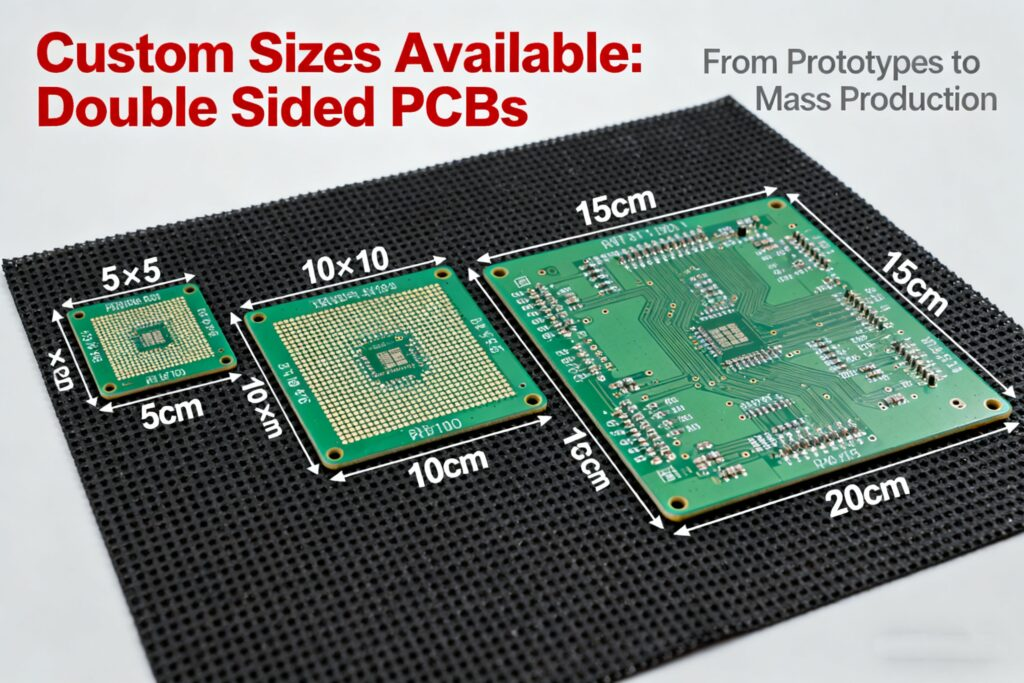
PCB Panelization: How Utilization Changes Unit Price
A PCB is priced on a panel, not on a board. The quote you receive is the panel price divided by the number of good boards on that panel, so the array — not…
2026.10.22 -
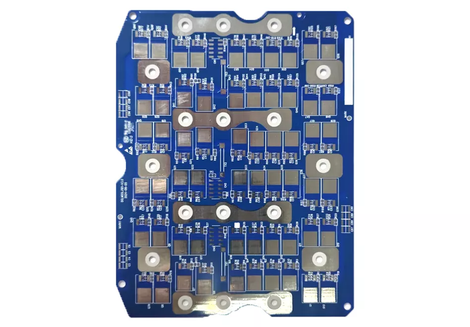
Heavy Copper PCBs: Etching, Solder Mask, and Thermal
Standard PCB copper is 1 oz, about 35 µm after plating. Heavy copper starts at 2 oz and can go to 10 oz or more, and it changes almost every process step: etching, plating,…
2026.10.22 -
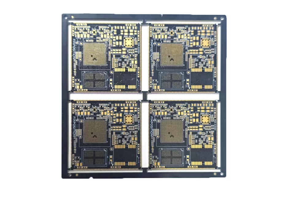
Backdrilling High-Speed PCBs: Stub, Cost, and DFM
A plated through hole is drilled through the entire board, but a high-speed signal usually uses only part of it. The unused copper below the signal layer is a stub, and at multi-gigabit rates…
2026.10.22 -
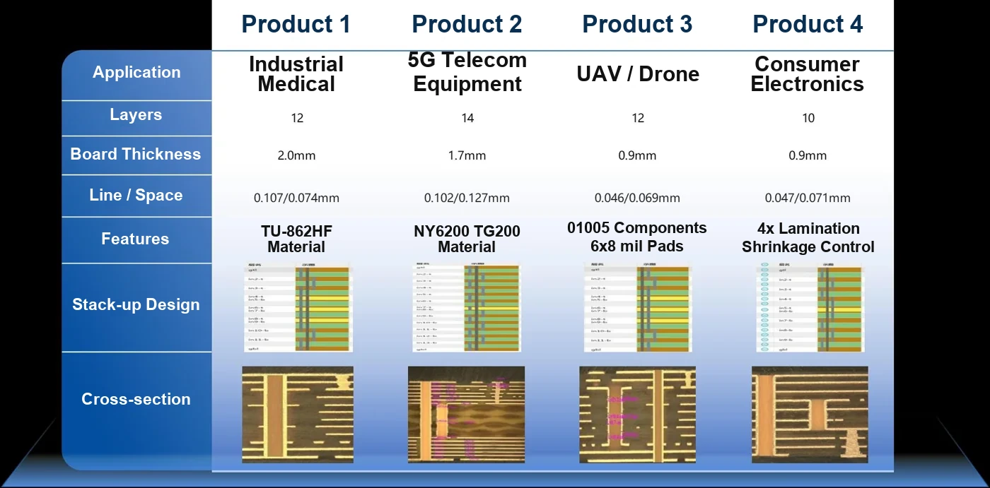
Blind, Buried, and Microvias: Cost and Reliability
A through via is the default. It is drilled after lamination, plated in one pass, and inspected like every other hole. Blind, buried and microvias break that simplicity: they require sequential lamination, extra drilling…
2026.10.22 -
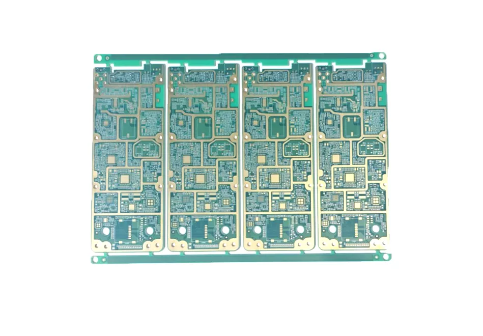
How to Count HDI Orders: 1+N+1, 2+N+2, 3+N+3
Two engineers can describe the same HDI board as "2-order" and "2+N+2" and still disagree about what will be built. One counts build-up layers per side, the other counts total build-up layers, and the…
2026.10.22