


Standard PCB copper is 1 oz, about 35 µm after plating. Heavy copper starts at 2 oz and can go to 10 oz or more, and it changes almost every process step: etching, plating, solder mask, lamination and thermal design.
The board is not simply a thicker version of a standard PCB. A design that works at 1 oz can be unmanufacturable at 4 oz because the minimum trace and space grow, the mask cannot cover the step, and the copper imbalance warps the panel.
This article covers what changes, where the limits are, and how to write a heavy copper stackup that a fabricator can build.
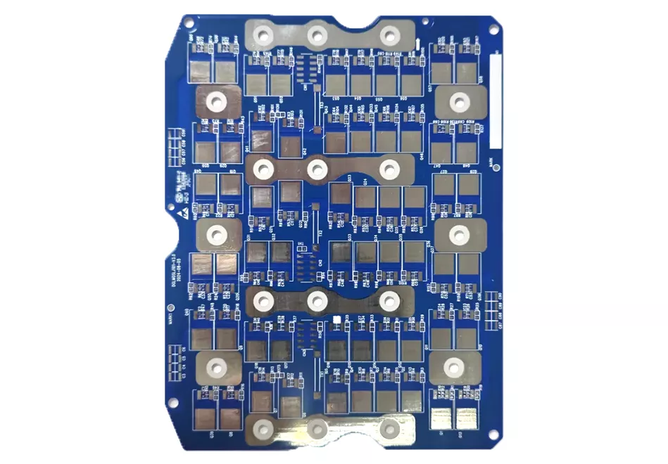
What counts as heavy copper
- 1 oz: 35 µm, standard.
- 2 oz: 70 µm, the entry point for power boards.
- 3–4 oz: 105–140 µm, common for motor drives and BMS.
- 6–10 oz: 210–350 µm, for high-current busbars and welding equipment.
The copper weight can be on the outer layers only, on inner layers, or on both. Each choice changes the process and the cost.
Etching thick copper
Etching removes copper from the surface to form traces. With thick copper, the etchant has to work longer and sideways as well as down, which produces undercut. The result is a trace that is narrower at the top than at the bottom, and a thickness tolerance that is wider than on 1 oz.
Practical consequences:
- Minimum trace and space increase with copper weight.
- Fine pitch components become difficult or impossible.
- The trace profile is trapezoidal, not rectangular.
- Impedance control is less precise.
A typical starting point is 0.20 mm trace and space at 4 oz, 0.25 mm at 6 oz and 0.30 mm at 10 oz. The exact limit depends on the fabricator's etch line and the pattern density.
Plating and solder mask
Heavy copper on the outer layers means a large step between copper and laminate. Solder mask has to cover that step without thinning at the edge or trapping solvent.
Problems that appear:
- Thin mask at the top edge of a thick trace.
- Bubbles or voids where the mask bridges a gap.
- Mask cracking after thermal cycling.
- Uneven color and thickness across the board.
The fabricator may need multiple mask coats, a slower cure, or a different mask type. The design should keep mask dams wide enough to cover the step and avoid mask over very sharp copper edges.
Thermal behavior
Heavy copper is usually chosen for one of two reasons: current carrying capacity or heat spreading.
For current, the trace width and copper weight are chosen from the allowable temperature rise. For heat, the copper spreads heat from a hot component to a larger area, and thermal vias move it to another layer.
Two design points matter:
- Copper balance. Heavy copper on one side and little on the other warps the board. Balance the copper or add thieving.
- Thermal relief. A thick copper plane conducts heat away from a solder joint, which can make hand soldering difficult. Thermal relief spokes help.
If the thermal path is the main requirement, an insulated metal substrate (IMS) board may be a better choice than heavy copper FR4. The two solve different problems: IMS spreads heat through the metal base, heavy copper spreads it in the plane.
DFM rules for heavy copper
- Keep the minimum trace and space inside the fabricator's qualified range for the copper weight.
- Avoid fine-pitch components on the heavy copper layer unless the fabricator confirms the etch capability.
- Balance copper across the board, or expect warpage.
- Design mask dams at least as wide as the copper step.
- Use thermal relief on through-hole pads connected to heavy planes.
- Specify the copper weight per layer, not only "heavy copper".
- Allow for a wider copper thickness tolerance and state it on the drawing.
Cost drivers
| Copper weight | Etch difficulty | Typical application | Cost index |
|---|---|---|---|
| 1 oz | Standard | General electronics | 1.0 |
| 2 oz | Moderate | Power supply, LED | 1.2–1.4 |
| 4 oz | High | Motor drive, BMS | 1.5–1.9 |
| 6–10 oz | Very high | Busbar, welding, high current | 2.0–3.0 |
The index is relative and depends on pattern density and layer count. The main drivers are etch time, plating time, mask coats and yield.
FAQ
Can I use 4 oz copper on a 0.1 mm trace?
No. The etch undercut and thickness tolerance make it unreliable. The minimum trace grows with copper weight.
Is heavy copper the same as thick copper?
The terms are used interchangeably. Both usually mean 2 oz or more.
Does heavy copper replace a heat sink?
It spreads heat, but it does not remove it from the board. A heat sink or metal base is still needed for high-power parts.
Can heavy copper be combined with HDI?
It is possible but uncommon. The build-up dielectric and laser drilling are not designed for thick copper steps. Review the stackup with the fabricator first.
What to send for a heavy copper review
- Copper weight per layer
- Current and allowable temperature rise
- Minimum trace and space
- Component pitch and thermal relief requirements
- Warpage or flatness requirement
- Acceptance class
Send your stackup for a heavy copper review, or review our metal core capability and multilayer capability.
Reviewed by the Benchuang process engineering team.