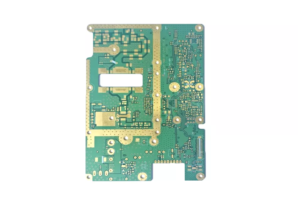



RF PCB Material and Stack-Up Requirements
An RF PCB quotation should identify the exact laminate maker and grade, the Dk/Df basis used in the design, copper type and roughness requirement, resin system, finished thickness and tolerance, and any approved substitution rules. Material trade names alone are not enough because construction, test method and operating-frequency context affect how the electrical data are interpreted.
For hybrid constructions, provide the exact material pair, thicknesses, copper, press requirements and reliability criteria. Material availability and any proposed substitution must be confirmed before production.
RF and High-Frequency PCB Manufacturing Capabilities
| Parameter |
Prototype/Sample |
Production |
| Available material categories |
FR-4 / M2 / M4 / M6 / M7 |
FR-4 / M2 / M4 / M6 |
| Controlled-impedance tolerance |
±9% |
±10% |
| Minimum inner-layer line/space |
45/45 µm |
45/50 µm |
| Minimum outer-layer line/space |
45/45 µm |
45/50 µm |
| Inner-layer copper range |
0.33–5 oz |
0.33–4 oz |
| Outer-layer copper range |
0.33–5 oz |
0.33–5 oz |
| Backdrill depth tolerance |
±0.05 mm |
±0.10 mm |
| Residual stub for board thickness ≤2.2 mm |
0.05–0.15 mm |
0.05–0.20 mm |
| Maximum production panel size |
600 × 400 mm |
600 × 400 mm |
| Surface finish options |
ENIG, OSP, OSP + ENIG, ENEPIG, plated gold fingers |
Same options |
| Special process options |
POFV, countersink, backdrill, castellated/half holes, side plating |
Available by design review |
Capability combinations depend on the complete board design. Final manufacturability is confirmed after reviewing the laminate, stack-up, copper, trace geometry, via transitions, panel layout and order quantity.
Controlled Impedance and RF Geometry
Single-ended and differential impedance targets must be tied to the approved stack-up, reference planes, trace width and spacing, finished copper and test method. Manufacturing review covers etch compensation, registration, dielectric and copper consistency, coupon requirements and final inspection. The agreed construction and test plan should be released together with the board data.
Via Transitions and Backdrilling
Plated through-hole stubs, layer transitions, via placement and ground-via fences can influence high-frequency structures. When backdrilling is required, identify the target layer, residual-stub requirement, board thickness and inspection method. The engineering team checks these requirements during CAM and stack-up review before confirming the production plan.
Manufacturing Controls and Inspection
Relevant manufacturing controls include material verification, imaging and etch compensation, layer registration, copper and dielectric consistency, surface finish and dimensional inspection. Available inspection resources include impedance testing, AOI, electrical testing, metallographic inspection and environmental/reliability equipment. Required coupons, reports and acceptance criteria should be defined in the quotation package.
Typical RF and High-Frequency PCB Applications
- Mobile and data communication equipment
- High-speed networking and intelligent terminals
- Automotive electronics requiring controlled transmission structures
- Aerospace and industrial control projects subject to project qualification
Information Needed for an RF PCB Quotation
- Gerber, ODB++ or IPC-2581 data, NC drill files and fabrication drawing
- Exact laminate maker/grade, stack-up and Dk/Df design basis
- Copper specification, finished thickness and impedance table
- Frequency context, surface finish and via/backdrill requirements
- Quantities, testing requirements, target date and destination
RF PCB lead time is confirmed after material availability, stack-up, engineering questions, panel layout and testing requirements are agreed.
Why Work with Benchuang for RF PCBs
Benchuang combines PCB manufacturing, CAM/DFM review, controlled-impedance support and inspection resources for RF and high-frequency projects. Manufacturing is carried out at our Meizhou production facility, while the Shenzhen team coordinates overseas quotations, technical communication and export support. Exact materials and performance requirements are handled against the released project data, giving buyers a clear route from feasibility review to production.
Learn more about Benchuang, review our PCB services, or contact our team.
RF PCB FAQ
What information is required for an RF PCB quotation?
Provide board data, drill files, fabrication drawing, exact laminate and stack-up, Dk/Df basis, copper, thickness, impedance, frequency context, finish, via requirements, quantities and testing requirements.
Can Benchuang work with customer-specified high-frequency laminates?
Yes. Submit the exact laminate maker, grade, construction and substitution rules. The engineering team will confirm material availability and manufacturing feasibility for the project.
How is controlled impedance confirmed?
The engineering team checks the stack-up, trace geometry, copper assumptions, reference planes and requested test method. The capability table lists ±9% for prototype/sample and ±10% for production.
Why do Dk, Df and copper roughness matter?
These inputs affect the customer's transmission and loss model. Provide the exact design basis and material test method so fabrication is aligned with the released electrical design.
When is backdrilling required?
Backdrilling may be specified when plated through-hole stubs need to be reduced. The target layer, board thickness, residual-stub requirement and inspection method must be included in the fabrication data.
Which surface finish should be selected?
The finish depends on assembly, contact, geometry, storage and electrical requirements. Available options include ENIG, OSP, OSP plus ENIG, ENEPIG and plated gold fingers.
Can RF and FR-4 materials be combined?
A hybrid stack-up can be evaluated from the exact material pair, thickness, copper, press conditions and reliability requirements. Material compatibility must be confirmed before production.
What determines RF PCB lead time?
Material availability, stack-up approval, engineering-question closure, panel layout, fabrication complexity and testing requirements determine the confirmed schedule.