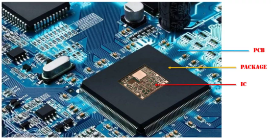




Equipment control boards, evaluation boards, test interfaces and package substrates are different products. Conventional PCB capability does not automatically establish suitability for a package substrate or fine-pitch interposer. Define the board role, device interface, electrical targets and mechanical constraints before manufacturing feasibility is confirmed.
Engineering Review Points
- Interface: supply package, socket, connector or contact geometry, pin assignments and alignment requirements. Test interfaces may need controlled contact finish, planarity and repeatable positioning.
- Routing: release layer architecture, feature sizes, microvia spans and via treatment. Review dense escape routing with pad geometry, registration and assembly requirements.
- Electrical performance: identify impedance, loss, current and isolation targets with the measurement method. Include sockets, connectors and vias when evaluating the complete interface.
- Qualification: define thickness, flatness, temperature and contact cycles. Package substrates need explicit package-assembly, warpage and qualification requirements, confirmed independently from ordinary PCB fabrication.
Prepare Your Project Files
Provide fabrication and drill data, stack-up, interface drawings and acceptance specifications. Include BOM, assembly files, electrical tests, fixtures and traceability where relevant. State whether the request is for equipment electronics, a test board or package substrate, with quantities and qualification timing.