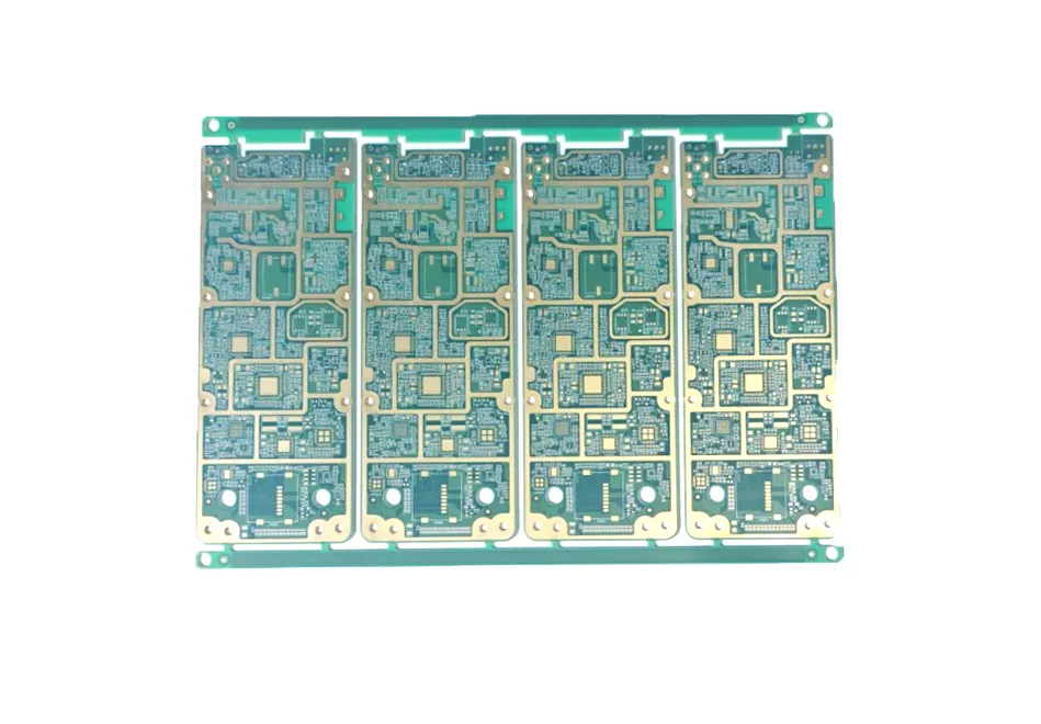
HDI PCB Construction Options
Benchuang supports 1-step, 2-step and 3-step HDI constructions. A 1-step structure uses one sequentially laminated microvia build-up on each applicable side of the core. Additional build-up cycles provide more microvia transition levels for higher routing density. Registration, copper balance, dielectric selection, resin flow and via-to-pad geometry become increasingly important as the number of HDI build-up steps increases.
Blind vias connect an outer layer to one or more inner layers, buried vias connect internal layers, and plated through holes connect the full board thickness. Stacked and staggered microvias can both be evaluated. The correct arrangement depends on routing, capture-pad geometry, filling and plating requirements, reliability targets and the complete stack-up.
HDI PCB Manufacturing Capabilities
| Parameter |
Prototype/Sample |
Production |
| Maximum layer count |
32 layers |
18 layers |
| Finished board thickness |
Up to 6.0 mm |
Up to 2.8 mm |
| Minimum dielectric thickness |
0.060 mm |
0.064 mm |
| Available material categories |
FR-4 / M2 / M4 / M6 / M7 |
FR-4 / M2 / M4 / M6 |
| Minimum blind-via drill diameter |
0.060 mm |
0.075 mm |
| Minimum buried-via drill diameter |
0.10 mm |
0.15 mm |
| Minimum through-hole drill diameter |
0.15 mm |
0.15 mm |
| Maximum plated through-hole aspect ratio |
14:1 |
10:1 |
| Maximum laser-via aspect ratio |
1:1 |
0.8:1 |
| Minimum inner-layer line/space |
45/45 µm |
45/50 µm |
| Minimum outer-layer line/space |
45/45 µm |
45/50 µm |
| Controlled-impedance tolerance |
±9% |
±10% |
| Minimum drill/pad |
0.12/0.25 mm |
0.15/0.30 mm |
| Maximum production panel size |
600 × 400 mm |
600 × 400 mm |
| Surface finish options |
ENIG, OSP, OSP + ENIG, ENEPIG, plated gold fingers |
Same options |
| Special process options |
POFV, countersink, backdrill, castellated/half holes, side plating |
Available by design review |
Capability combinations depend on the complete board design. Final manufacturability is confirmed after reviewing the files, stack-up, material, copper, via structure, panel layout and order quantity.
Microvia, Stack-Up and Impedance Engineering
A reliable HDI quotation starts with the target stack-up and impedance table. Dielectric thickness, copper distribution, reference-plane continuity, material selection and finished copper affect achievable trace geometry. For each microvia, identify the drill type, finished diameter, capture pad, target layer and whether the structure is stacked or staggered. Resin filling and plated-over-filled-via (POFV) requirements should also be identified in the fabrication data.
Controlled impedance is checked against the confirmed stack-up, trace geometry, copper assumptions and agreed test method. Where coupons or specific reports are required, include them in the quotation package so inspection and documentation can be planned before production.
DFM and Quality Control for HDI PCBs
HDI design-for-manufacturability review covers line/space against copper weight, annular ring, drill-to-copper clearance, registration, via aspect ratio, resin filling, capture-pad geometry, copper balance and board thickness. The goal is to identify manufacturability and reliability risks before the production data are released.
Available inspection resources include automated optical inspection (AOI), X-ray-related inspection, electrical testing, impedance testing, metallographic inspection, thermal shock and environmental/reliability equipment. The inspection plan and required reports are agreed according to the project specifications.
Typical HDI PCB Applications
- Mobile and data communication hardware requiring compact routing and fine-pitch interconnection
- Automotive electronics and intelligent terminals with limited board area
- Industrial control and security electronics requiring multilayer interconnection
- Aerospace and other space-constrained electronic assemblies subject to project qualification
HDI PCB Prototype and Pilot Lead Times
Typical production-cycle targets after file and material confirmation are 8–12 days for a 1-step HDI sample and 10–15 days for a pilot run; 13–15 days for a 2-step sample and 16–18 days for a pilot run; and 15–17 days for a 3-step sample and 19–21 days for a pilot run. Engineering-question time, material waiting and legal holidays are excluded. The confirmed schedule is issued after the files, materials, panel layout and testing requirements are agreed.
Information Needed for an HDI PCB Quotation
- Gerber, ODB++ or IPC-2581 data, NC drill files and fabrication drawing
- Layer count, dimensions, finished thickness, material and target stack-up
- Blind, buried and through-via structure; stacked/staggered and filling requirements
- Copper weights, surface finish, impedance table and required test method
- Prototype, pilot or production quantities, target date and destination
Why Work with Benchuang for HDI PCBs
Benchuang has focused on advanced multilayer and HDI PCB manufacturing since 2007. HDI production is carried out at our Meizhou facility, supported by laser drilling, sequential lamination, imaging, inspection and reliability resources. Our Shenzhen team coordinates overseas quotations, technical communication and export support. Buyers receive one project path from initial DFM review through prototype, pilot and production planning.
Learn more about Benchuang, review our PCB services, or contact our team.
HDI PCB FAQ
What HDI build-up levels can Benchuang manufacture?
Benchuang supports 1-step, 2-step and 3-step HDI structures. The final lamination cycles and microvia transitions are confirmed from the stack-up and design files.
What are the minimum blind-via sizes?
The minimum blind-via drill diameter is 0.060 mm for prototype/sample work and 0.075 mm for production. Final feasibility depends on the stack-up, capture pad, copper and aspect ratio.
Can Benchuang manufacture stacked and staggered microvias?
Both structures can be evaluated. Provide the layer transitions, capture-pad geometry, filling/plating requirements and reliability criteria so the sequential lamination plan can be confirmed.
What files are required for an HDI PCB quotation?
Provide Gerber, ODB++ or IPC-2581 data, NC drill files, fabrication drawing, stack-up, material, copper, via structure, impedance table, finish, quantities and testing requirements.
How do copper weight and line/space affect manufacturability?
Heavier copper requires more etch allowance and can limit fine conductor geometry. Line/space, copper weight, via dimensions and registration are therefore checked together during DFM review.
Which surface finishes are available?
Available options include ENIG, OSP, OSP plus ENIG, ENEPIG and plated gold fingers. The choice depends on assembly, contact, storage and project requirements.
How is controlled impedance handled?
The engineering team checks the stack-up, trace geometry, copper assumptions, reference planes and requested test method. The capability table lists ±9% for prototype/sample and ±10% for production.
What affects HDI lead time?
Build-up steps, material availability, microvia architecture, engineering-question closure, panel layout, special processes and testing requirements affect the confirmed schedule.