



Via-in-pad is now routine on HDI boards. A via that sits inside a component pad has to be filled, cured and planarized before the pad can be plated and soldered. If the resin contains a void, the pad may look flat and still collapse in reflow, wick solder into the hole, or crack after thermal cycling.
Voids in plugged vias are a process-capability problem, not a cosmetic one. This article covers why they form, how to measure them, what to put in the specification, and where X-ray stops being enough.
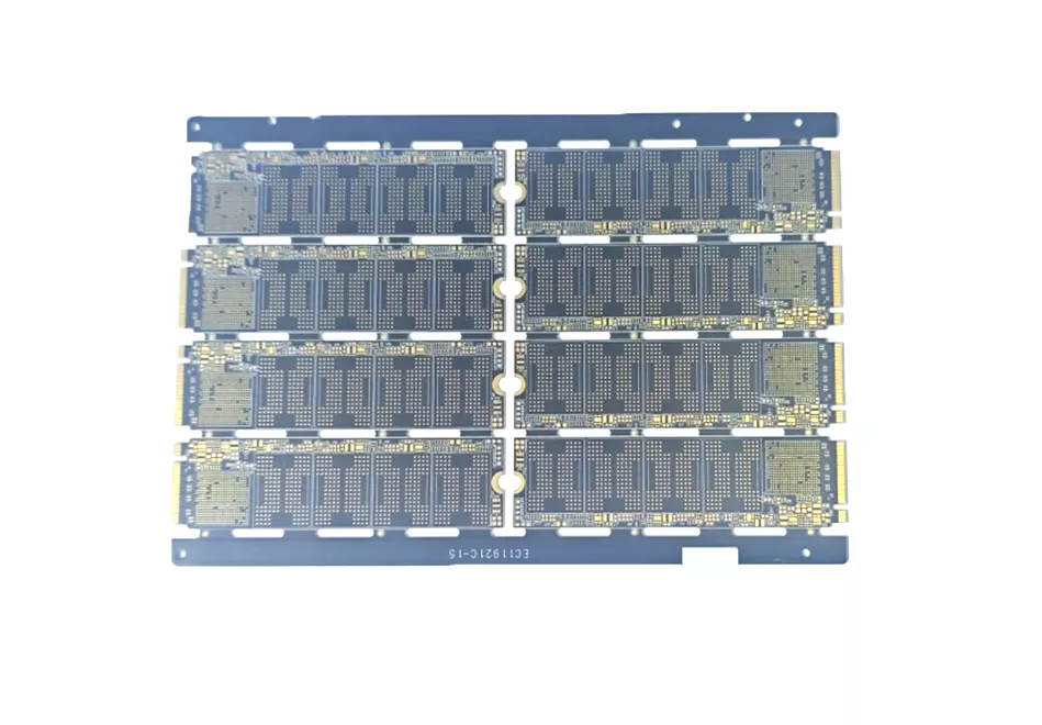
What a plugged via is
A plugged via is a through, blind or buried via filled with resin and, in most via-in-pad designs, capped with copper. IPC-4761 describes several protection types:
- Type II: via plugged with resin, not covered.
- Type V: via filled, not covered.
- Type VI: via filled and covered.
- Type VII: via filled and capped, with the cap plated and planarized for soldering.
Via-in-pad normally requires Type VII. The distinction matters because a Type V fill can leave a dimple that traps flux, while a Type VII cap must be flat enough to place a paste deposit.
Why voids form
1. Resin viscosity and de-airing
Plugging resin is a filled epoxy. If the filler settles or the resin is not de-aired before use, air remains in the syringe or the container and ends up in the via. Viscosity that is too high prevents the resin from reaching the bottom of a small hole.
2. Plugging method and pressure
Screen, stencil and roller plugging each push resin differently. A single pass from one side often leaves a void at the far end of the hole. Vacuum-assisted plugging removes air ahead of the resin and is the usual choice for high-aspect-ratio vias.
3. Hole geometry and wall quality
A rough wall, a barrel with a step, or a drill smear pocket gives the resin a place to bridge over instead of fill. The void then sits against the wall, where thermal cycling concentrates stress.
4. Cure shrinkage
Epoxy shrinks as it cures. A fast cure can shrink the resin away from the wall or leave a dimple at the surface. The cure profile has to be qualified for the specific resin thickness, not copied from a different board.
5. Planarization and capping
Grinding or plasma planarization can open a void just below the surface. If the cap copper is then plated over it, the void is hidden until reflow or cross-section. Cap thickness and surface flatness belong in the same specification as the void limit.
How to measure voids
X-ray is fast and useful for a first look at large voids and fill coverage. It is not an acceptance test on its own:
- It projects the whole barrel, so small voids near the wall can be hidden by copper above and below.
- It cannot measure cap thickness or resin recession.
- It cannot confirm bond to the wall.
Use X-ray for screening and cross-section for acceptance. Section the vias at the highest aspect ratio, at the smallest drill, and at the panel edge. Measure void area as a percentage of the via cross-section, note the position (center or wall), and record cap copper thickness at the same location.
Acceptance criteria
The numbers below are a starting point for a purchase specification. They must be agreed with the fabricator and tied to the IPC-4761 type and the end use.
| Characteristic | Suggested limit | Method |
|---|---|---|
| Void area in plugged via | ≤ 5% of via cross-section | Cross-section |
| Void at via wall | Not permitted | Cross-section |
| Dimple depth after planarization | ≤ 25 µm | Cross-section or optical |
| Cap copper thickness | Per drawing, typically ≥ 25 µm | Cross-section |
| Resin recession | No gap between resin and wall | Cross-section |
| Delamination after thermal stress | None | Thermal stress + cross-section |
Two rules make these limits usable. First, define how many vias are sectioned and where. Second, define what happens when a void is found: rework, scrap or concession. Without those two rules the limit is only a number on a drawing.
Process controls that matter
- De-air and store resin according to the supplier's pot life and viscosity data.
- Use vacuum-assisted plugging for vias above the agreed aspect ratio.
- Qualify the cure profile on the actual resin volume and board thickness.
- Control drill quality: a smeared or stepped wall will produce voids regardless of the resin.
- Measure cap thickness and dimple depth at first article and at each resin lot change.
- Keep cross-section images with the lot record.
What to ask your supplier
- Which IPC-4761 type do you use for via-in-pad, and how is it verified?
- What is the void acceptance limit, and how many vias are sectioned per panel?
- Is plugging vacuum-assisted, and what is the aspect ratio limit?
- How is the cure profile qualified when resin lot or board thickness changes?
- What happens to the panel if a void is found?
FAQ
Can a void be seen on X-ray?
Large voids, yes. Small voids at the wall and thin caps usually require a cross-section.
Is a 5% void acceptable?
It depends on the via function, the IPC-4761 type and the customer standard. A void at the wall is treated more severely than a centered void. Put both the limit and the measurement method in the drawing.
Does a void always cause a field failure?
No, but it removes the margin. Under thermal cycling or reflow, a void can grow into a crack or allow solder to wick into the barrel.
Can plugged vias be reworked?
Rework is limited and usually means drilling out and re-plugging before final plating. After cap plating, a defective via generally means scrapping the piece.
What to send for a DFM review
- Stackup with via types and IPC-4761 callouts
- Via table with drill size, aspect ratio and via-in-pad locations
- Cap copper and surface finish requirements
- Thermal cycling or reflow profile
- Acceptance standard and sampling plan
Send your via-in-pad stackup for review, or review our HDI capability and HDI manufacturing page.
Reviewed by the Benchuang process engineering team.

