




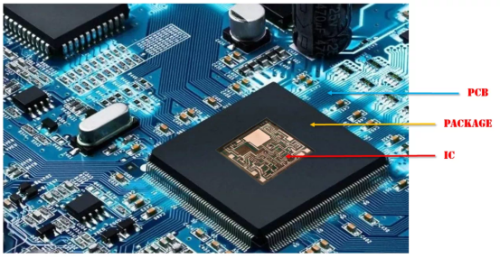
A chip, package and PCB are three different levels of an electronic assembly. The chip performs the electrical function, the package protects the die and adapts its very small connections to an assembly footprint, and the PCB routes power, signals and grounds between packaged devices. Treating these as interchangeable components leads to late footprint, thermal or manufacturability problems.
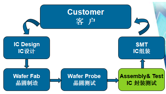
Chip vs. Package vs. PCB: What Each Part Does
An integrated circuit (IC) chip is fabricated on a semiconductor die. It contains the transistors and other circuit elements that perform logic, processing, power management or another defined function. The die is the functional core, but it is not normally connected directly to a conventional PCB.
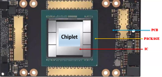
An IC package provides mechanical protection, environmental protection, electrical connection and a practical thermal path. It also transforms the die's fine-pitch bonding points into external pins, leads, pads or solder balls that an assembly process can place and solder reliably.
A printed circuit board (PCB) is the interconnect platform. Its copper layers route signals between the package and other components, while planes and vias distribute power and ground. The PCB must also support the package footprint, assembly clearances, inspectability and the expected heat load.
| Level | Primary job | What the project team must define |
|---|---|---|
| IC die | Performs the circuit function inside the semiconductor | Function, electrical limits, heat generation and die-level connection requirements |
| Package | Protects the die and provides an assemblable electrical interface | Package family and drawing, pinout, land pattern, thermal path, MSL and handling requirements |
| PCB | Connects packaged devices and provides mechanical support | Stack-up, trace and spacing, via structure, impedance, thermal design, footprint and test access |
How the Package Connects a Chip to the PCB
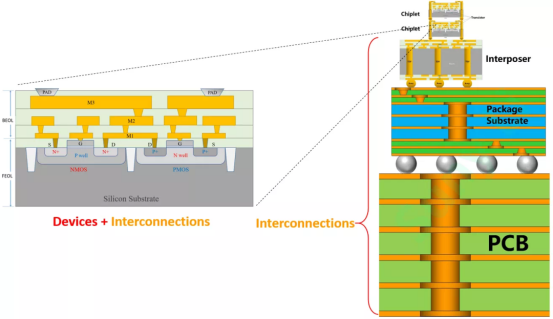
Inside the package, wire bonds or flip-chip interconnects link the die to an internal substrate or leadframe. Those connections are routed to the package's external solder features. The PCB then uses its own copper and via structure to carry the signals to connectors, passive components and other ICs.
The package therefore sits between two connection scales. Its die-side features are extremely fine, while its board-side pitch is large enough for stencil printing, placement and reflow. The board footprint should be taken from the qualified package drawing rather than copied from an unverified third-party library.
Four Main Functions of an IC Package
1. Mechanical and electrical connection
Leads, pins, pads or solder balls establish a repeatable interface with the PCB. Package materials and lead finishes also affect soldering, reliability and the permitted assembly process.
2. Physical protection
The package body protects the fragile die and its internal interconnects from particles, handling damage, contamination and mechanical stress. The required protection level depends on the product environment and assembly route.
3. Heat transfer
Packages create a thermal path from the die to the board, a heat spreader, a thermal pad or the surrounding air. Exposed pads and thermal vias can help conduct heat into the PCB, but copper area, via placement, solder voids and the enclosure layout must be evaluated together.
4. Environmental protection
Molding compounds, lids, underfill and other package materials help protect the die from moisture and contamination. Moisture sensitivity, storage, baking and reflow limits should be confirmed before components are released to assembly.
How Package Choice Changes PCB Design and Assembly
The package family affects far more than the footprint. A QFN may require thermal-pad and solder-void control; a BGA may require via-in-pad or dog-bone fanout decisions, X-ray inspection and careful warpage control; a fine-pitch package may require tighter stencil apertures and placement accuracy. These are project-specific decisions, not generic rules for every package.
Before release, verify the package drawing, land pattern, pin numbering, paste layer, courtyard, keep-outs, reference designators, component height and polarity. Also check stencil thickness, placement data, reflow profile, inspection method and rework access. Close package and PCB footprints against the manufacturer's current revision rather than relying only on the CAD library name.
For package-level substrates with fine lines, build-up layers or dense microvias, review the process separately through IC substrate PCB manufacturing requirements. When conventional board routing requires microvias or high-density fanout around the package, compare the HDI PCB manufacturing guide.
Information to Check Before PCB Fabrication and Assembly
- The approved PCB revision, stack-up, Gerber and drill data match one another.
- Every package footprint matches the current datasheet and package drawing.
- Assembly drawings identify polarity, orientation, nozzle clearance and keep-out areas.
- The BOM, approved manufacturer parts and approved alternatives are complete.
- The thermal plan is consistent with package power, copper area, via placement and enclosure conditions.
- The inspection and test plan covers solder joints, thermal pads and package-specific risks.
For projects that include fabrication, component sourcing, SMT and test, use the turnkey PCB and PCBA service. To request a technical review, send the PCB files, BOM, placement data, assembly drawing, package list, quantity and target date through the Benchuang contact page. Manufacturing and assembly decisions are confirmed after review of the actual project package.