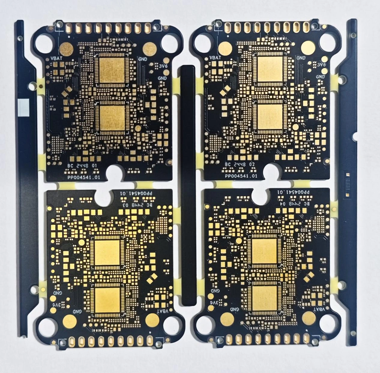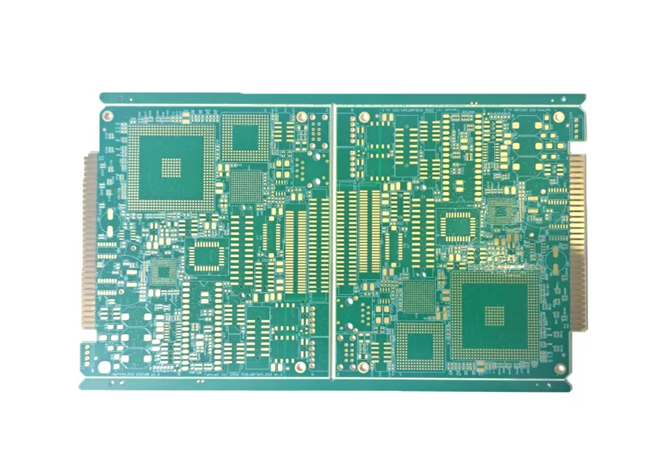



AI server boards are not just dense; they are thick. A GPU carrier or switch board can run 20 to 30 layers, with backdrilled vias, low-loss laminate and strict impedance control.
At that layer count, yield is decided before fabrication: by stackup symmetry, material choice and how the vias are designed. A board that is theoretically routable can still be unmanufacturable at acceptable yield.
This article covers what changes above 20 layers and where to focus.
Why layer count grows
- High-speed lanes need reference planes and routing space.
- Multiple power rails need plane pairs.
- Backdrilling removes stubs but adds process steps.
- Fine-pitch packages need escape routing on several layers.
Each added layer adds a lamination cycle, a registration step and a chance for warpage.
Material choices
| Requirement | Material direction | Note |
|---|---|---|
| Low loss at 25–56 Gbps | Low-Df laminate | Df 0.002–0.004 |
| Thermal reliability | High Tg (170 °C+) | Lead-free assembly |
| CTE match | Low-CTE laminate | Fewer barrel cracks |
| CAF resistance | CAF-resistant core | Dense via fields |
| Warpage control | Symmetrical stackup | Balanced copper |
Mixing materials is common: low-loss for high-speed layers, standard FR-4 for control layers. Each interface is a process risk and must be reviewed.
Stackup rules
- Keep the stackup symmetrical around the center to reduce warpage.
- Balance copper on both sides of each layer pair.
- Keep dielectric thickness consistent for impedance.
- Put high-speed layers next to a solid reference plane.
- Define backdrill layers and stub targets before quoting.
- Use the same material for layers that share a via.
Yield levers
Registration. With 20+ layers, layer-to-layer registration errors accumulate. The fabricator's registration capability sets the minimum annular ring and the via pad size.
Lamination. More cycles mean more chances for voids and delamination. Press parameters and material cure must match.
Drilling. Aspect ratio grows with thickness. A 3 mm board with a 0.25 mm hole is 12:1; deeper holes plate less uniformly.
Backdrilling. Removing stubs on a thick board requires depth control and inspection. It is a yield risk, not only a cost.
Warpage. Thick boards with asymmetric copper warp during assembly. Specify flatness and check first article.
DFM rules
- Keep the aspect ratio inside the fabricator's qualified range.
- Avoid stacking more than two blind/buried via levels without review.
- Define the backdrill depth and tolerance per via type.
- Specify impedance coupons for each high-speed layer.
- Allow for a wider bow and twist tolerance on thick boards.
- Review panel size; a large board may not fit the press or the assembly line.
FAQ
Can any fabricator build 20+ layers?
No. It requires registration, lamination and drilling capability that not every shop has. Ask for the qualified layer count.
Is backdrilling always needed above 20 layers?
Not always, but high-speed lanes usually need it. The stub length matters more than the layer count.
Does a thicker board cost more?
Yes. More material, more cycles and lower yield all add cost. The price is not linear with layer count.
What is the biggest yield risk?
Registration and warpage. Both are decided by the stackup and the fabricator's process, not by the layout alone.
Layer count is the least interesting number on an AI server board. What decides whether it builds is registration, lamination and warpage. Send the stackup and the target yield, and we will tell you which of the three is the constraint.