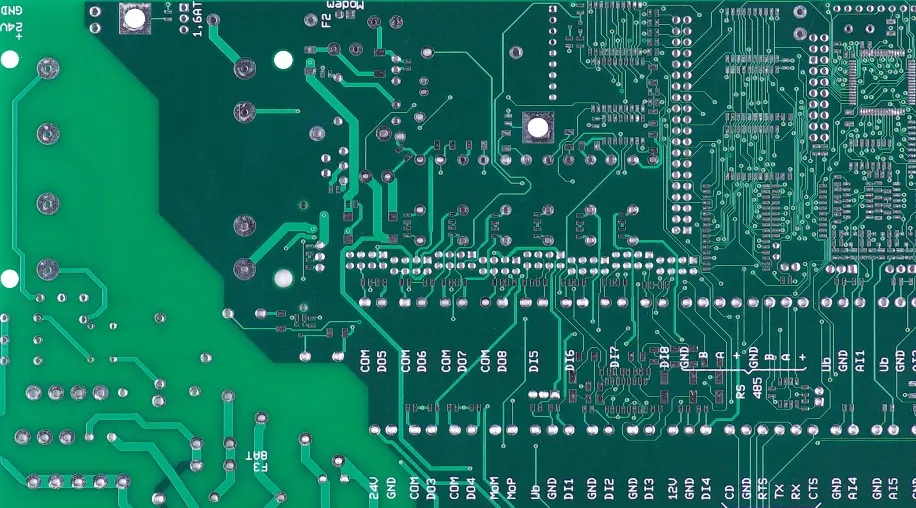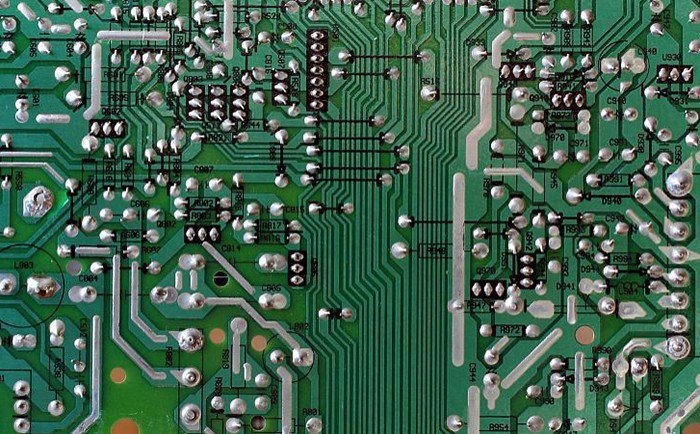



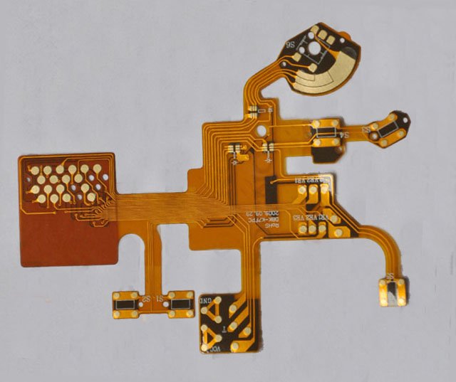
Flexible printed circuits (FPCs) use flexible dielectric materials, commonly polyimide, with copper conductors. Rolled-annealed or electrodeposited copper and adhesive-based or adhesiveless laminates are selected according to the construction and bending requirements. Due to their high flexibility, lightweight and compact design, bendability, and foldability, they are widely used in electronic products such as mobile devices, automotive electronics, medical equipment, and aerospace applications.
The FPC flexible circuit board manufacturing process involves subjecting the FPC substrate to a series of processing steps to create conductive layers, insulating layers, and interlayer connectors, thereby producing a flexible board with circuit functionality that is both bendable and foldable.
1. FPC design and layout.
Designers create the FPC circuit diagram based on actual requirements, determining parameters such as the routing, width, and spacing of conductive traces. During layout, considerations include the required electronic components and the stacking sequence of different material layers.
2. Conductive layer fabrication.
The copper conductor layer may use rolled-annealed or electrodeposited foil selected for the flex construction and application. Through processes such as photolithography and etching, the conductor layer patterns are formed on the conductive layer. Subsequently, an electroplating process is performed to coat the surface of the conductor layer with a protective layer of metallic material.
3. Insulation Layer Manufacturing.
The insulation layer serves to isolate and protect the conductor layer. The most commonly used insulating layer material is polyimide film, which can be applied using layered or localized adhesive methods. Cutting processes are used to cut the film into the desired shape and position it to align with the conductor layer.
4. Hole-punching process.
Holes may be formed mechanically or by laser according to their purpose and the construction. A hole alone does not connect layers: electrical vias require a conductive interconnect process such as metallization and plating.

5. Cover layer processing.
The cover layer is used to provide overall protection for the FPC circuit, preventing physical damage from external sources. Common cover layer materials include photosensitive adhesives and coating adhesives. Through lamination, the cover layer is bonded to the FPC substrate layer, ensuring a tight and secure connection.
6. Surface treatment process.
Through chemical or mechanical processing, oxides and contaminants are removed from the FPC surface to enhance the reliability and stability of circuit connections.
BenChuang Electronics produces customized Flexible PCB boards. Contact us and send your specifications.