Custom Flexible PCB Manufacturer for Prototype and Production
Flexible PCB manufacturability depends on the complete stack-up, copper construction, coverlay, stiffeners, bend zones, interfaces and assembly conditions. Shenzhen Benchuang Precision Electronics Co., Ltd. confirms materials, manufacturing limits and test coverage only after reviewing the released project data.
Flexible PCB Reference Specifications for Quotation
The following figures are reference ranges for preparing an initial FPC quotation. They describe possible product configurations, not guaranteed combinations on every design. Confirm the released stack-up, material grade, copper, coverlay, bend condition, panel size and acceptance criteria through project-specific DFM before order release.
Parameter
Reference range
Quotation check
Layer count
1 to 16 layers
Confirm copper stack-up, bonding method and bend-zone layer count.
Finished thickness
0.06 to 0.40 mm
Specify whether coverlay, adhesive and stiffener are included in local thickness.
Minimum line / space
0.045 / 0.045 mm
Check copper type, finished copper and etch compensation together.
Minimum mechanical drill
0.10 mm
Identify drilled versus finished hole diameter and layer span.
Copper foil options
12 / 18 / 35 / 70 um
Confirm rolled-annealed or electrodeposited copper where flex reliability requires it.
Stiffener options
FR-4 / PI / PET / stainless steel / PSA
Specify material, thickness, adhesive, outline and position.
Panel-size reference
Single/double layer: up to 250 by 4000 mm; multilayer: up to 500 by 750 mm
Actual usable area depends on bend direction, tooling, material roll and panel yield.
For RFQs, include Gerber or ODB++ data, drill files, a layer stack-up, bend drawing, stiffener and coverlay details, quantity and required inspection documents. For assembly support, see PCB assembly services.
Flexible PCB Construction and Design Inputs
A flexible PCB, also called a flex PCB or FPC, uses a flexible dielectric and copper circuitry so the finished circuit can fold or bend into the product. Manufacturing decisions depend on whether the circuit bends only during installation or moves repeatedly during operation. The released data should identify the layer count, dielectric and adhesive construction, copper type and weight, finished thickness, bend zones, stiffener locations, contact areas and dimensional datum system.
Routing through a bend zone should be reviewed together with the bend direction, radius, angle and expected motion. Trace width, spacing, copper grain direction, coverlay openings, transition geometry and local thickness changes can affect strain. Dynamic-flex requirements must include the intended cycle target and test method; they cannot be inferred from the outline alone.
Flexible PCB Project Parameters
Flexible PCB capability depends on the complete construction and use condition. Final manufacturability is confirmed after reviewing the released stack-up, material, copper, bend requirements, coverlay, stiffeners, panel layout and order quantity.
Project input
What the buyer should specify
Construction and layer count
Specify single-layer, double-layer or multilayer flex and release the intended stack-up.
Flexible dielectric
Specify polyimide or other required flexible dielectric, maker/grade when mandatory, and thickness.
Copper construction
Specify copper type and weight; review them with bend mode, trace geometry and finished thickness.
Coverlay
Define coverlay thickness, adhesive, openings, registration and permitted squeeze-out.
Stiffeners
Define material, thickness, adhesive, location, datum and interface requirements.
Bend mode
State installation/static or dynamic use, bend radius, angle, direction, cycle target and test method.
Connector/contact areas
Provide pad or finger geometry, dimensions, surface finish and mating requirements.
Controlled impedance
Provide target, tolerance, layer/reference-plane relationship and test-coupon method.
Panel and profile
Define panel format, tooling, routing/laser cutting, fiducials and delivery format.
Inspection and acceptance
Define electrical, dimensional and visual checks plus coverlay, stiffener and impedance criteria when required.
Capability combinations depend on the complete board design. Final manufacturability is confirmed after reviewing the stack-up, material, copper, via structure, panel layout and order quantity.
Bend Zones and Conductor Routing
The bend definition is a manufacturing input, not only a mechanical drawing note. Mark each bend zone, bend line and bend direction, and identify whether the circuit will be bent once during installation or repeatedly in service. The review should consider routing direction, trace transitions, copper balance, local openings and the distance between holes, pads, stiffeners and the bend area.
For dynamic motion, avoid relying on a generic bend-cycle claim. Provide the assembly condition, bend radius, travel, speed, temperature range, cycle target and acceptance method so material and conductor construction can be evaluated against the actual application.
Coverlay, Stiffeners and Connector Interfaces
Coverlay protects the copper and defines exposed pads, but its adhesive flow and opening registration must suit the pad geometry. Stiffeners may support connectors, components or contact fingers and can use different materials and thicknesses according to the interface. The fabrication drawing should show stiffener outlines, datum features, adhesive requirements, keep-outs and finished local thickness.
Contact areas need the exact surface finish, pad or finger dimensions, plating length and any bevel or mating requirement. If the flex circuit is assembled to rigid boards, connectors or components, provide the assembly drawing and identify handling, flatness and tooling needs before panelization is approved.
Manufacturing, Assembly and Quality Control
Flexible PCB fabrication includes imaging and etching of the copper circuitry, drilling and plating where required, coverlay registration and lamination, surface finish, stiffener bonding, profiling, electrical testing and final inspection. DFM review checks minimum geometry, annular rings, copper balance, coverlay openings, adhesive flow, local thickness, outline tolerances and panel handling.
For assembled flex projects, provide the BOM, centroid/pick-and-place data, assembly drawing, approved component substitutions, special process instructions and test requirements. Component support, reflow exposure, tooling, connector areas and final handling should be reviewed with the bare-board construction rather than after fabrication is released.
Representative Flexible PCB Samples
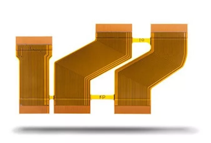
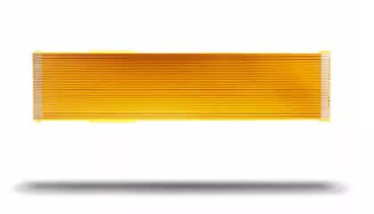
Representative two-layer flexible PCB sample using Shengyi SF-305 material and ENIG surface finish. This is sample evidence, not a blanket material or process limit.Representative two-layer flexible PCB sample with plated gold and nickel finish. Any detailed material string or 0.30 +/- 0.05 mm thickness is sample-specific only.
Typical Flexible PCB Applications
Compact consumer and mobile electronics
Camera, display and connector modules
Industrial sensors and compact control assemblies
Communications equipment and wearable electronics
Automotive and medical electronics subject to project-specific qualification
Information Needed for a Flexible PCB Quotation
Gerber, ODB++ or IPC-2581 data, NC drill data and a dimensioned fabrication drawing
Layer count, released stack-up, base material, copper construction and finished thickness
Static/installation or dynamic bend definition, bend zones, radius, direction and test requirement
Coverlay, stiffener, adhesive, connector/contact and surface-finish requirements
BOM, centroid data, assembly drawing and test requirements when PCBA is required
Prototype, pilot or production quantity, target date and shipping destination
Describe the key requirements in the Message field. After the inquiry is received, our team will confirm the file-transfer method for the complete technical package.
Send Your Flexible PCB Project Details
Include the layer count, stack-up, bend requirements, coverlay or stiffener details, quantity and target date. Our team will confirm the file-transfer method for the complete technical package.
Why Work with Benchuang for Flexible PCBs
Benchuang combines PCB manufacturing with engineering review for stack-up, bend zones, coverlay, stiffeners, surface finish and assembly interfaces. Founded in 2007, the company operates a Meizhou manufacturing center and supports overseas quotations, technical communication and export coordination through its Shenzhen team. Prototype, pilot and production requirements are reviewed against the same released technical package, helping buyers control changes as the project moves toward volume production.
Frequently Asked Questions
Is a flex PCB the same as a flexible printed circuit or FPC?
Yes. Flex PCB, flexible printed circuit and FPC are commonly used for a circuit made on a flexible dielectric. The correct fabrication route still depends on the layer construction, copper, coverlay, stiffeners and intended bending condition.
What files are required for a flexible PCB quotation?
Provide Gerber, ODB++ or IPC-2581 data, NC drill files, a fabrication drawing and the released stack-up. Include bend zones, coverlay, stiffeners, surface finish, quantities and assembly data when PCBA is required.
What is the difference between static and dynamic flex?
A static or installation flex is normally bent during assembly and then remains in position. A dynamic flex moves repeatedly in service, so the bend radius, travel, speed, cycle target, temperature and test method must be defined.
How is the minimum bend radius determined?
It is evaluated from the complete construction and use condition, including layer count, dielectric, adhesive, copper type, finished thickness, trace routing and whether the motion is static or dynamic. Benchuang does not apply one universal radius to every design.
What is the difference between coverlay and solder mask?
Coverlay is a flexible film-and-adhesive construction commonly used to protect flex circuitry and define openings. The correct opening, registration and adhesive-flow rules should be released in the fabrication data.
When are stiffeners required on a flexible PCB?
Stiffeners are often used under connectors, components, contact fingers or other areas needing mechanical support or controlled local thickness. Their material, outline, thickness, adhesive and datum must be specified.
Can a flexible PCB include controlled impedance?
Yes, when the stack-up, reference planes, trace geometry, finished copper, target and tolerance are defined. The complete construction and test-coupon method must be reviewed before the production stack-up is released.
Can Benchuang support flexible PCB prototypes and assembly?
Benchuang can review prototype, pilot, production and PCBA requirements. For assembly, include the BOM, centroid data, assembly drawing, component rules and test requirements with the bare-board package.