


An AI-generated PCB layout is only as production-ready as the constraints, stack-up and release package behind it. A routed database can be electrically complete while remaining unsuitable for the selected lamination cycle, microvia structure, impedance build, copper distribution, panel format or test strategy.
Benchuang is currently testing AI-assisted layout workflows within its existing DFM and CAM process. We do not apply a separate manufacturing standard to an AI PCB layout. The released data is reviewed against the same material, imaging, drilling, plating, filling, impedance, electrical-test and assembly controls used for conventionally routed HDI and multilayer boards.
For an experienced engineering team, the relevant question is therefore not whether an AI tool can complete the routing. It is whether the released database closes every interface between design intent, PCB fabrication, assembly and production verification.

The Release Problem Is Constraint Closure, Not Routing Origin
For complex boards, PCB layout best practices are not a collection of generic routing tips. They are the controlled alignment of electrical constraints, material selection, manufacturing tolerances, mechanical interfaces and test requirements.
An automated placement or routing result can comply with the wrong rule set. Before the layout is treated as releasable, the project team should be able to identify:
- the approved stack-up revision;
- the source and owner of each net-class rule;
- the manufacturing rule profile loaded into the design database;
- the approved via definitions and layer spans;
- room-specific, component-specific and local routing overrides;
- which footprints, constraints or stack-up values were generated automatically;
- which exceptions remain subject to engineering review.
Where constraint definition, placement or routing completion is still part of the project scope, it should be handled separately through defined PCB layout design services. Fabrication DFM should not be used to reconstruct incomplete electrical design intent after release.
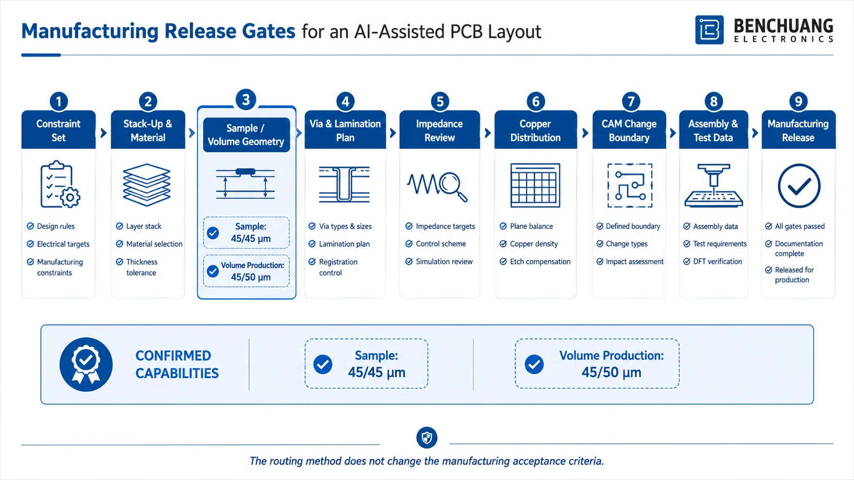
| Release Gate | Data That Must Be Frozen | Typical Risk if Left Open |
|---|---|---|
| Constraint set | Net classes, current rules, spacing, keep-outs and approved exceptions | The layout passes DRC against rules that do not match the production process |
| Stack-up | Core, prepreg, copper, finished thickness, material family and lamination sequence | Impedance and via geometry are based on a nominal rather than producible build |
| Geometry | Sample or volume-production rule set | Prototype-limit features are carried into repeat production without review |
| Via architecture | Layer spans, drill type, pad geometry, filling and stacking method | Routing creates an unnecessary lamination cycle or an unqualified microvia stack |
| Controlled impedance | Target, tolerance, reference layer, finished copper and coupon requirement | Trace geometry no longer matches the released production stack-up |
| Copper distribution | Plane structure, local density, current paths and heavy-copper regions | Resin-fill, flatness, etching or thermal risks appear at panel level |
| Flex mechanics | Bend area, bend direction, coverlay, stiffener and local thickness | The circuit is electrically correct but mechanically unsuitable |
| CAM authority | Permitted compensation and changes requiring an EQ | Manufacturing adjustments alter controlled design intent |
| Assembly and test | BOM, CPL, drawings, programming and test requirements | The bare board revision does not match the assembly release |
1. Lock the Stack-Up Before Treating Trace Geometry as Final
A layer count and finished board thickness do not define a production stack-up. Before critical routing is frozen, the stack-up should identify the actual core and prepreg construction, pressed dielectric thickness, base and finished copper, resin demand, glass style where relevant, material family, acceptable substitutions and sequential-lamination stages.
For high-speed and RF-related structures, the review should also identify the Dk and Df basis, copper profile, solder-mask condition and any insertion-loss requirement. A nominal dielectric value entered into the layout database is not sufficient if the selected material, test method or pressed thickness changes during production planning.
The same applies to mixed copper weights, asymmetric constructions and high-layer-count boards. Material availability and press construction should be closed before the final trace geometry is approved, particularly when the layout contains impedance-controlled escape regions or narrow local neck-downs.
For projects requiring stack-up and lamination review, the released construction should be checked against the actual multilayer PCB manufacturing route rather than a generic EDA stack-up template.
2. Separate Sample Capability From Volume-Production Rules
AI-assisted routing frequently seeks the smallest permitted geometry to increase route completion. That approach is only valid when the rule set represents the intended production stage.
Benchuang’s current line-and-space capability is separated as follows:
| Geometry Item | Sample Build | Volume Production |
|---|---|---|
| Minimum inner-layer line / space | 45 / 45 μm | 45 / 50 μm |
| Minimum outer-layer line / space | 45 / 45 μm | 45 / 50 μm |
These figures define process capability boundaries; they are not a universal routing grid for every board. Approval still depends on base copper, finished copper, feature distribution, conductor length, etch compensation, impedance class, panel utilization and the yield target for the order.
A sample build may use 45/45 μm geometry after project review, while the corresponding production release must be checked against the 45/50 μm volume rule. Where the production dataset retains prototype-limit features, they should be identified explicitly rather than left as unrecorded local exceptions.
The same distinction should be applied to hole structures, annular rings, solder-mask bridges, finished-hole tolerances, backdrill requirements and aspect ratios. A proper PCB engineering and DFM review should state which features are standard production rules, which are approved exceptions and which remain subject to engineering evaluation.
3. Convert HDI Routing Into a Defined Lamination and Via-Fill Plan
For an HDI design, a completed route is not a complete manufacturing definition. Every blind, buried and laser-drilled via must be translated into a documented lamination route.
The via table should identify:
- start and end layers;
- mechanical, buried or laser-drilled via type;
- nominal drill and finished-hole requirements;
- capture-pad and target-pad geometry;
- stacked, staggered or skip-via arrangement;
- via-in-pad, copper filling and capping requirements;
- dielectric thickness for each laser-drilled span;
- the associated sequential-lamination stage.
An AI PCB layout may reduce local routing distance by adding microvias or changing layer transitions. That optimization can also introduce another lamination cycle, a difficult stacked-via structure, tighter registration demand or additional filling and planarization requirements.
The review therefore needs to follow the full manufacturing sequence: inner-layer imaging and AOI, lamination, X-ray registration, laser drilling, copper deposition and plating, via filling, outer-layer imaging, impedance verification and electrical testing. Local route efficiency should not be evaluated independently from the complete HDI process route.
Projects using microvias, sequential lamination, via-in-pad or filled and capped structures should be submitted for an HDI PCB manufacturing review before the layer transitions are frozen.

4. Close Impedance Against the Production Stack-Up
Controlled-impedance data should be tied to the released stack-up revision rather than stored only as nominal rules in the layout database.
The impedance table should define:
- the controlled net or net class;
- single-ended or differential target;
- permitted tolerance;
- routing layer and reference plane;
- target line width and differential spacing;
- finished copper and solder-mask condition;
- coupon and test-report requirements;
- approved neck-down regions and escape exceptions.
BGA escape geometry deserves separate treatment. A short local neck-down may be electrically and manufacturably acceptable, but it should not be hidden inside a general differential-pair rule. The location, length and impedance expectation of the exception should be stated.
Layer transitions should also be reviewed for return-path continuity, reference-via placement, plane splits and via stubs. Where backdrilling is required, the drill side, target layer, residual stub requirement and depth tolerance must be included in the fabrication data.
Any rerouting performed after field-solver or stack-up closure should trigger a check of the affected impedance structures. Passing the original DRC does not confirm that the modified route still matches the production calculation.
5. Review Copper Distribution at Panel Level
Automated layout optimization is normally performed at board level. Lamination, imaging, etching, plating and flatness are controlled at both board and production-panel level.
The review should examine:
- copper balance between corresponding layers;
- local copper density around dense BGAs and connector areas;
- resin demand around planes, thermal pads and via arrays;
- large isolated copper-free regions;
- mixed inner- and outer-layer copper weights;
- heavy-current paths and current carried through vias;
- POFV or filled-via areas that affect local planarization;
- the interaction between copper distribution and bow or twist.
Copper thieving and normal CAM compensation can improve panel behavior, but they cannot correct a fundamentally unbalanced construction without affecting the original layout. Where copper balance conflicts with RF clearance, creepage, thermal or current requirements, the decision should be resolved by engineering rather than left to automatic CAM adjustment.
6. Add Flex and Rigid-Flex Mechanical Constraints to the Release
For flexible and rigid-flex products, the design package must define the physical construction in addition to the electrical database. Coverlay, adhesive, copper, base film and stiffener are functional parts of the released structure, not purchasing details to be decided after routing.
The project data should identify:
- static installation bending or repeated dynamic flexing;
- bend direction, bend radius and required cycle life;
- copper type and grain-direction requirements where applicable;
- coverlay construction and opening tolerances;
- stiffener material, location, thickness and adhesive;
- exposed-finger, connector and local-thickness requirements;
- component, via and pad restrictions within active bend areas;
- rigid-to-flex transition-zone geometry.
For rigid-flex boards, the rigid and flexible regions must be reviewed as one lamination structure. Layer numbering, flex cores, coverlay termination, no-flow or bonding materials, local thickness and transition geometry must agree across the stack-up drawing, Gerber data, drill files and mechanical drawing.
A route can be electrically valid while placing vias, pad transitions or abrupt conductor-width changes in a mechanically unsuitable area. Those conditions will not be resolved by a standard rigid-board DRC profile.
7. Define the CAM Change Boundary Before EQ Review
The fabrication drawing should define which manufacturing compensations are permitted and which changes require customer approval. This prevents routine CAM preparation from being confused with electrical redesign.
| CAM or Process Item | May Be Covered by Documented Fabrication Rules | Normally Requires Customer EQ |
|---|---|---|
| Etch compensation and pad scaling | Yes, when performed within agreed finished dimensions and impedance controls | When the change alters a controlled electrical or mechanical feature |
| Drill-tool grouping | Yes, when finished-hole size, tolerance and annular ring remain compliant | When the finished hole or pad relationship changes |
| Solder-mask and legend cleanup | Yes, if allowed by the fabrication notes and no functional opening is changed | When component, test-point or coating requirements may be affected |
| Material or stack-up substitution | No, unless a standing approved-alternative rule exists | Yes, particularly for impedance, RF, thermal or reliability-controlled builds |
| Microvia span, fill or stacking change | No | Yes |
| Controlled-impedance geometry change | Only within an agreed impedance-compensation process | Yes, for neck-down, spacing, reference-layer or topology changes |
| Copper removal or addition | Only non-functional thieving under agreed rules | Yes, when current, shielding, return path or thermal behavior may change |
| Panelization change | Yes, for standard rails and coupons when permitted | When edge connectors, break-off stress or assembly fixtures are affected |
For AI-assisted databases, this boundary is particularly important because automatically generated geometry may not include documentation explaining why a local exception exists. CAM should not infer electrical intent from the visual appearance of the layout.
8. Close Assembly and Test Data Against the Same PCB Revision
The Gerber or ODB++ package, NC Drill files, BOM, centroid file, assembly drawing and test plan must use the same revision and reference-designator set.
The assembly release should confirm:
- footprint-to-part-number agreement;
- pin-one and polarity orientation;
- exposed-pad and paste-coverage requirements;
- component height and mechanical keep-outs;
- global and local fiducials;
- tooling holes, rails and panel orientation;
- inspection requirements for BGA, QFN and hidden joints;
- ICT, flying-probe or functional-test access;
- programming interfaces and firmware revision;
- coating, potting and depanelization restrictions.
DFT access cannot normally be recovered during bare-board CAM preparation. If the automated placement process consumes test-point or probe access, that conflict should be resolved before the PCB release rather than after the first assembly build.
Automatically created or substituted footprints also need direct verification against the actual ordered component. Package family, pitch and body dimensions alone do not confirm pad geometry, exposed-pad design, polarity or assembly compatibility.
9. Treat Sample Concessions as Controlled Deviations
Rapid automated iteration can create multiple internally valid versions of the same design. Manufacturing should receive one controlled release package with an identified revision, not a combination of files collected from separate exports or email attachments.
The EQ record should show:
- the issue and affected layer, net or component;
- the proposed manufacturing or design change;
- the responsible approver;
- the approved revision;
- whether the decision applies only to the sample build or also to volume production;
- the date the issue was closed.
A successful sample build does not automatically approve all sample concessions for volume production. Where 45/45 μm sample geometry was accepted, the production release must still be checked against the 45/50 μm volume rule and the agreed production stack-up, copper condition and process route.
Prototype inspection results, impedance data, microsections, assembly findings and functional-test results should be incorporated into the volume release. The manufacturer should not be required to reconstruct the approved production configuration from an earlier quotation, EQ thread and prototype data set.
Release Package for Manufacturing Review
| File or Data | Required Information |
|---|---|
| Gerber, ODB++ or IPC-2581 | One complete and controlled PCB layer package |
| NC Drill and rout data | Plated, non-plated, blind, buried, backdrill, slot and profile definitions |
| Fabrication drawing | Dimensions, tolerances, finish, marking, acceptance criteria and special processes |
| Stack-up | Materials, core/prepreg construction, copper, dielectric thickness and lamination stages |
| Impedance table | Net class, target, tolerance, routing layer, reference layer and coupon requirement |
| Via table | Layer spans, drill type, diameter, pad geometry, fill, cap and stack arrangement |
| IPC-356 or netlist data | Independent connectivity verification where available |
| BOM and approved alternatives | Manufacturer part number, substitution policy and critical-component restrictions |
| CPL and assembly drawing | Reference designators, coordinates, rotations, polarity and mechanical requirements |
| Test and programming plan | Inspection, ICT/FCT, firmware, test fixtures and acceptance requirements |
| Project stage and quantity | Sample, pilot or volume-production status and required delivery schedule |
Frequently Asked Questions
Does an AI PCB layout require a different DFM standard?
No. The manufacturing acceptance criteria should remain the same. Stack-up, material, geometry, hole structure, impedance, copper distribution, assembly data and test requirements must be reviewed regardless of whether the layout was completed manually, through conventional autorouting or with AI assistance.
Can 45/45 μm sample geometry be released directly for volume production?
Not automatically. Benchuang’s current minimum line-and-space capability is 45/45 μm for sample builds and 45/50 μm for volume production, on both inner and outer layers. The volume release must be reviewed against the production rule, copper condition, feature distribution and agreed process route.
Should the PCB manufacturer be told that AI was used?
The routing method does not change the manufacturing criteria. However, the design owner should identify automatically generated footprints, stack-ups, constraints or local routing decisions that have not been independently verified. This helps separate confirmed design intent from provisional tool output.
What should be frozen before automated placement or routing?
At minimum, freeze or formally control the board outline, component interfaces, stack-up direction, material assumptions, net classes, controlled-impedance requirements, via definitions, current rules, mechanical keep-outs, flex zones and test-access strategy. Routing generated before these inputs are stable is likely to require substantial rework.
Can CAM engineering correct an AI-generated PCB layout?
CAM can apply documented production compensation such as approved etch allowance, drill grouping, rout compensation and non-functional cleanup. Changes to electrical topology, impedance geometry, via spans, materials, current paths, return paths or mechanical interfaces require an EQ and customer approval.
Order & Project Support
For an AI-assisted or conventionally routed project, provide the controlled PCB data, drill files, stack-up, impedance table, via table, fabrication drawing, BOM, placement data, assembly drawing, quantities and project stage. The review can then identify manufacturing conflicts, open engineering decisions and any differences between sample and volume-production rules.