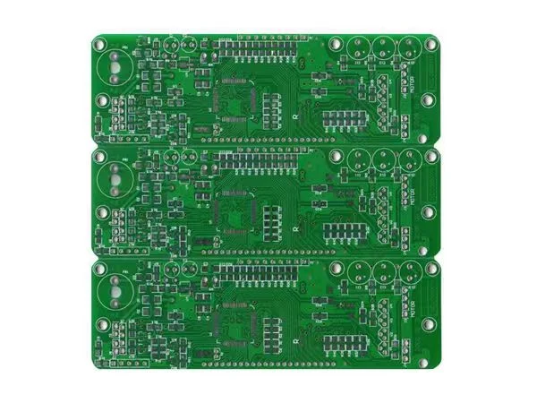
When a Double-Sided PCB Is the Right Choice
A 2-layer board is often suitable for moderate routing density, cost-sensitive control boards, power and LED control, industrial electronics, communication products and consumer electronics. Both copper sides can carry routed connections, and plated through holes provide electrical connection between them. Compared with a single-sided board, this provides more routing flexibility without adding internal layers.
When to Consider a 4-Layer PCB
A 4-layer construction may be a better choice when return-path continuity, electromagnetic interference control, controlled impedance, routing density, multiple power domains, thermal distribution or component placement cannot be handled cleanly on two layers. The decision should consider board performance, layout effort, manufacturability and total project cost rather than layer count alone.
Double-Sided PCB Manufacturing Capabilities
| Parameter |
Prototype/Sample |
Production |
| Construction |
2-layer rigid PCB with plated through holes |
2-layer rigid PCB with plated through holes |
| Finished board thickness |
Up to 6.0 mm |
Up to 2.8 mm |
| Minimum through-hole drill diameter |
0.15 mm |
0.15 mm |
| Maximum plated through-hole aspect ratio |
14:1 |
10:1 |
| Outer-layer copper range |
0.33–5 oz |
0.33–5 oz |
| Minimum outer-layer line/space |
45/45 µm |
45/50 µm |
| PTH diameter tolerance |
±0.05 mm |
±0.076 mm |
| NPTH diameter tolerance |
±0.05 mm |
±0.05 mm |
| CNC profile tolerance |
±0.076 mm |
±0.10 mm |
| Warpage |
≤0.5% |
≤0.5% |
| Maximum production panel size |
600 × 400 mm |
600 × 400 mm |
| Surface finish options |
ENIG, OSP, OSP + ENIG, ENEPIG, plated gold fingers |
Same options |
| Special process options |
Countersink, castellated/half holes, side plating |
Available by design review |
| Typical production cycle |
5–6 days |
Pilot run: 7–8 days |
Capability combinations depend on the complete board design. Final manufacturability is confirmed after reviewing the dimensions, material, copper, drill requirements, surface finish, panel layout and order quantity.
Manufacturing Flow and DFM Review
A typical double-sided PCB process includes material cutting, drilling, plated through-hole processing, imaging and etching, solder mask, legend, surface finish, profiling, electrical testing and final inspection. DFM review checks board area, thickness, copper weight, minimum line/space, drill sizes, annular rings, slots, routing or V-score, panel utilization, finish and quantities.
Both copper layers are outer layers, so copper weight directly affects fine-line etching. Plated and non-plated holes must be identified separately, and outline complexity, castellations, edge plating and copper balance can affect panel design and handling.
Inspection and Quality Control
Available inspection resources include automated optical inspection (AOI), electrical testing, metallographic inspection, impedance testing when specified, gold/nickel thickness measurement, thermal shock and environmental test equipment. The required checks and reports are agreed according to the board specifications and order requirements.
Typical Double-Sided PCB Applications
- Industrial controllers and instrumentation
- Power supplies, LED control and general power electronics
- Communication and consumer electronic products
- Automotive and security electronics subject to project requirements
Lead Time and Quotation Information
For 2–4 layer through-hole boards, typical production-cycle targets after file and material confirmation are 5–6 days for prototypes and 7–8 days for pilot runs. Engineering-question time, material waiting and legal holidays are excluded. Final timing depends on data completeness, material, panel layout, finish, special processes, testing and order quantity.
- Gerber, ODB++ or IPC-2581 data, NC drill files and fabrication drawing
- Board dimensions, material, finished thickness and copper weight
- PTH/NPTH, slots, outline, routing or V-score and panel requirements
- Surface finish, solder mask, legend, impedance and special processes
- Prototype, pilot or production quantities, target date and destination
Why Work with Benchuang for Double-Sided PCBs
Benchuang supports double-sided PCB projects from DFM review and prototype through pilot and production planning. Manufacturing is carried out at our Meizhou production facility with drilling, plating, imaging, etching, surface finish and inspection resources. The Shenzhen team coordinates overseas quotations, technical communication and export support, giving international buyers one contact path throughout the order.
Learn more about Benchuang, review our PCB services, or contact our team.
Double-Sided PCB FAQ
Is a double-sided PCB the same as a 2-layer PCB?
Yes. Both terms normally describe a rigid board with two copper circuit layers, commonly connected by plated through holes.
When should a design move from 2 layers to 4 layers?
Consider four layers when return paths, EMI control, controlled impedance, routing density, power distribution, thermal requirements or component placement cannot be handled cleanly on two layers.
What are the minimum drill and line/space capabilities?
The minimum through-hole drill diameter is 0.15 mm. Minimum outer-layer line/space is 45/45 µm for prototype/sample and 45/50 µm for production, subject to copper, finish and design.
What copper weights are available?
The outer-layer copper capability range is 0.33–5 oz for prototype/sample and production. Fine line/space and heavy copper requirements must be evaluated together.
Which surface finishes are available?
Options include ENIG, OSP, OSP plus ENIG, ENEPIG and plated gold fingers. Selection depends on assembly, contact and storage requirements.
What information is needed for a quotation?
Provide board data, drill files, fabrication drawing, dimensions, material, thickness, copper, finish, profile, quantities, testing requirements, target date and destination.
What quality checks can be specified?
Available resources include AOI, electrical testing, metallographic inspection, impedance testing where specified, finish-thickness measurement and environmental equipment.
What affects prototype and pilot lead time?
File completeness, engineering-question closure, material, panel layout, finish, special processes, testing and quantity affect the confirmed schedule.