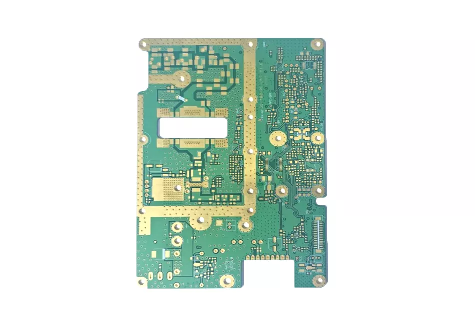
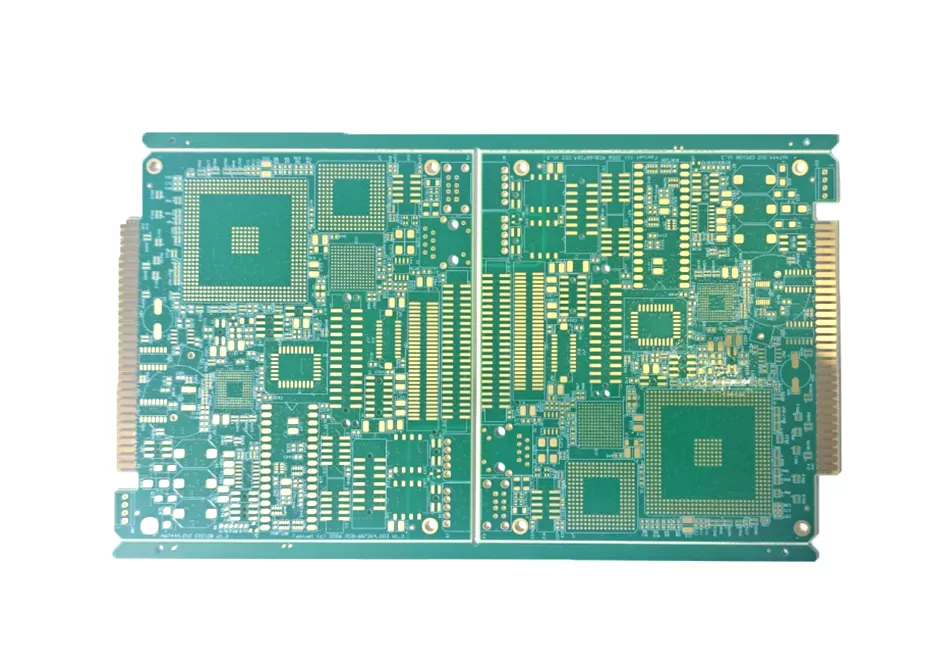
RF and microwave PCB performance is determined by the complete signal path, not by a laminate name or a maximum-frequency claim. The material system, stack-up, copper profile, transmission-line geometry, reference planes, launches, vias, grounding and fabrication tolerances must be reviewed together for the intended frequency range and loss budget. A manufacturable RF PCB specification therefore starts with measurable electrical targets and released design data.
RF PCB Quotation Parameter Checklist
Use this checklist to define the electrical, material, transition and verification requirements for a project review. These are buyer-supplied design targets, not blanket manufacturing limits; feasibility and test coverage are confirmed for the released stack-up and measurement method.
| Parameter | What to provide | Review point |
|---|
| Operating frequency | Frequency band, bandwidth and intended signal or antenna use | Dk/Df, impedance and loss targets must be evaluated at the relevant frequency. |
| Impedance targets | Single-ended or differential values, tolerance, layer and reference plane | Review with the released stack-up, trace geometry, finished copper and test coupon. |
| Loss and electrical limits | Insertion-loss or attenuation limit, test band and reference planes; include S-parameter requirements when applicable | Define fixture, calibration and measurement method before setting acceptance criteria. |
| Laminate and dielectric | Required maker and grade, Dk/Df source and test frequency, approved alternatives | Company portfolio material examples are project references; material suitability and availability need confirmation. |
| Stack-up and copper | Layer sequence, dielectric thicknesses, copper weights, reference planes and hybrid construction | Check impedance, loss, symmetry, lamination and material compatibility together. |
| Copper profile | Copper type/treatment and roughness requirement or approved material data | Roughness can affect high-frequency loss; identify the basis used in the design model. |
| Launches and transitions | Connector launch geometry, via spans, backdrill/residual-stub target, grounding and edge plating | Review the full signal path and define controlled features in the fabrication drawing. |
| Verification and acceptance | Coupon design, fixture, calibration, instrument/method, sample plan and pass/fail limits | RF performance claims require an agreed test setup and acceptance method. |
Documented High-Speed and Multilayer Material Examples
Benchuang's 2025 company portfolio documents multilayer builds using NY6200 TG200, TU-862HF and TU-872 SLK, and lists MEG6 material in high-speed PCB examples. These are project-specific manufacturing references; they do not by themselves establish RF insertion-loss, dielectric-constant or S-parameter performance for a new design. For an RF quotation, name the required laminate maker and grade or approve an equivalent only after reviewing the material data at the operating frequency.
Provide the frequency band, impedance targets and tolerances, maximum insertion loss or attenuation, copper roughness requirements, launch and connector details, via-transition strategy, test coupon, fixture and measurement method. The selected stack-up and any hybrid material construction must be checked against those requirements before release.
Material and Stack-Up Review
Laminate Dk and Df values must be interpreted at the relevant test method and frequency. Engineering review should also cover dielectric thickness, copper weight and roughness, resin system, material availability, hybrid-stack compatibility, thermal requirements and stack-up symmetry. Substituting a material without rechecking impedance and loss can change circuit behavior.
Impedance, Launches and Via Transitions
Controlled-impedance traces depend on the approved stack-up and finished copper geometry. Connector launches, coplanar ground spacing, reference-plane continuity, via transitions, ground stitching, cavities, edge plating and any backdrill requirement should be defined in the fabrication data. Trace width alone is not an adequate RF acceptance criterion.
Inspection and Test Coverage
Inspection and testing should match the project risk. The quotation can define electrical test, impedance coupons, dimensional and visual acceptance, registration checks, surface-finish requirements and RF measurements when a test method, fixture and acceptance limits are supplied. Frequency performance or insertion loss should not be implied when the required test setup is not defined.
Files for an RF PCB Quotation
Shenzhen Benchuang Precision Electronics Co., Ltd. reviews Gerber or ODB++ data, stack-up, impedance tables, fabrication drawings, material requirements, quantities and optional assembly files for custom RF PCB and PCBA projects. Materials, feature limits, tolerances, inspection, test coverage and delivery schedule are confirmed for the specific design before production.