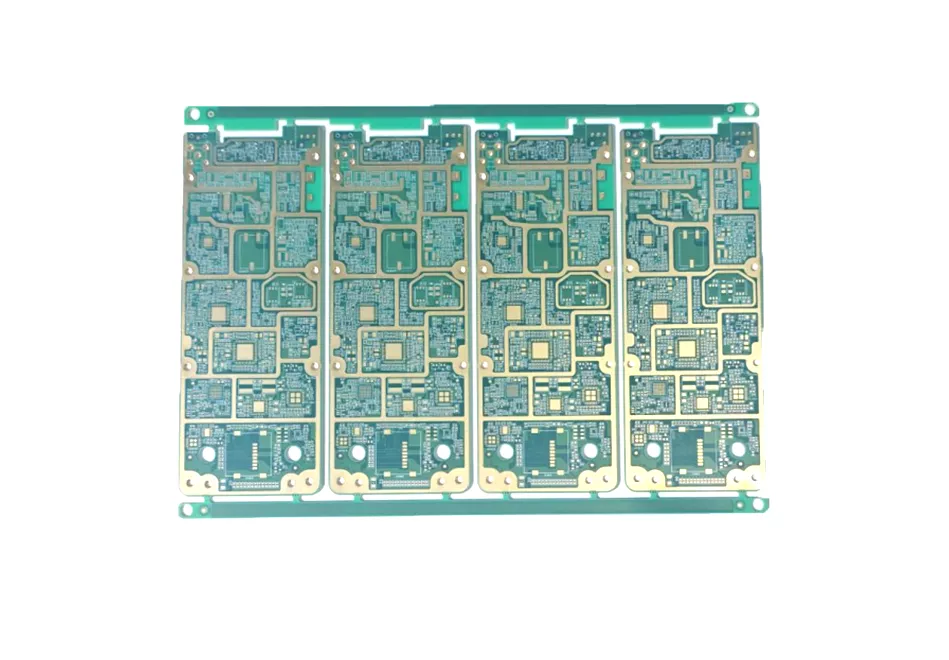
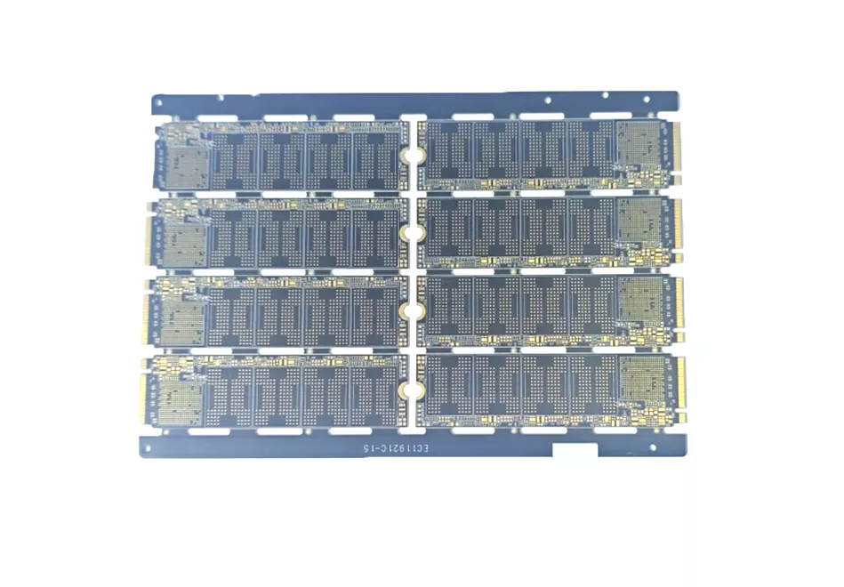
A high-density interconnect (HDI) PCB uses microvias, fine conductor geometry, reduced capture pads or sequential build-up structures to increase interconnection density. The benefit depends on the complete layout, stack-up, material system, signal requirements, assembly interface and qualification plan. HDI does not automatically reduce layer count or guarantee electrical or reliability performance.
Documented HDI Build Examples
The following entries are individual examples documented in Benchuang’s 2025 company profile. They show selected builds, not universal process limits; values from different projects should not be combined into one guaranteed specification.
| Application example | Layers | Finished thickness | Line/space | HDI / via detail |
|---|
| Smartwatch | 8 | 0.7 mm | 63/63 μm | 1-step build-up |
| 5G smartphone | 8 | 0.8 mm | 55/55 μm | 0.10 mm blind via |
| IoT device | 6 | 0.8 mm | 63/63 μm | 1-step; 0.10 mm blind via |
| Drone controller | 12 | 1.0 mm / 1.6 mm builds | 75/75 μm | 2-step; 0.10 mm blind via |
| Automotive multimedia | 10 | 1.6 mm | 75/75 μm | 3-step; 0.10 mm blind via |
Final feasibility depends on the released stack-up, material, copper, via structure, registration, finished dimensions, electrical targets, inspection plan and quantity. Please submit the complete project data for engineering review.
HDI Structure and Design Inputs
The released specification should define the layer architecture, build-up stages, microvia spans, finished thickness, material family, copper weight by layer, surface finish and solder mask. Any controlled-impedance, insertion-loss, current, thermal, mechanical or regulatory requirements should also be stated. The proposed construction and manufacturing route are confirmed only after the complete stack-up, drill data and design files are reviewed.
Microvia and Interconnect Review
Blind, buried, staggered, stacked or skip microvias and via-in-pad structures place different demands on lamination, drilling, plating and filling. Engineering review covers the layer span, dielectric thickness, laser feature and finished dimensions, capture pads, annular rings, aspect ratio, copper thickness, fill or cap specification and proximity to other vias and conductors. Feature limits depend on the complete combination, not one nominal diameter.
Sequential Lamination and Registration
Each build-up and lamination stage affects layer alignment, resin flow, dielectric thickness, copper balance and dimensional movement. Registration allowances and compensation are specific to the selected materials, panel format, copper distribution and number of process cycles. The sequence should be reviewed before tooling because a change in via span or layer relationship can change the entire process route.
Fine Routing and Controlled Impedance
Routing documentation should identify critical line and space, pad geometry, differential or single-ended impedance targets, tolerances, relevant layers and reference planes. Trace geometry is evaluated with dielectric thickness, copper thickness, solder mask, surface finish and material properties under the stated supplier test method. Where required, the quality plan can define stack-up approval, coupon design and measurement reporting.
Assembly, Inspection and Qualification
Via-in-pad and fine-pitch component interfaces may require defined filling, capping, planarity, pad finish, mask registration and cleanliness. The quality plan may include electrical test, automated optical inspection, dimensional and visual inspection, microsection review, X-ray inspection, impedance measurement and material documentation when specified. Thermal-stress or assembly-level qualification requires agreed samples, conditions, monitoring and failure criteria.
Files for an HDI PCB Quotation
Shenzhen Benchuang Precision Electronics Co., Ltd. reviews Gerber, ODB++ or IPC-2581 data, NC drill and laser data, stack-up, fabrication and mechanical drawings, microvia and filling requirements, impedance tables, quantities and optional assembly files for custom HDI PCB projects. Materials, manufacturing route, feature limits, inspection, qualification evidence, packaging and delivery schedule are confirmed for the specific design before production.