Multilayer PCB Manufacturer for Prototype and Production
Multilayer PCB performance depends on the complete stack-up, material system, copper distribution, lamination, registration, hole structures and acceptance criteria. Shenzhen Benchuang Precision Electronics Co., Ltd. confirms materials, manufacturing limits and test coverage only after reviewing the released project data.
Multilayer PCB Stack-Up and Material Review
A multilayer PCB combines outer and inner copper layers through one or more lamination cycles. The released stack-up should define core and prepreg construction, dielectric thicknesses, copper weights, finished thickness, material category, impedance relationships and any blind, buried or laser-via structure. Layer naming in the manufacturing data, stack-up drawing and impedance table must be consistent.
Material selection is reviewed against electrical performance, thermal requirements, finished thickness, copper and process route. Copper distribution and resin demand affect lamination, registration and flatness, so plane areas, heavy-copper regions and asymmetric constructions must be assessed before the panel plan is released.
Multilayer PCB Manufacturing Capabilities
Capability combinations depend on the complete board design. Final manufacturability is confirmed after reviewing the stack-up, material, copper, via structure, panel layout and order quantity.
POFV, countersink, backdrill, castellated/half holes, side plating
Available by design review
Lamination, Registration and Copper Balance
Multilayer fabrication requires consistent inner-layer imaging and etching, controlled oxide or bonding preparation, material lay-up, lamination and registration before drilling and plating. DFM review checks dielectric selection, resin demand, copper distribution, layer symmetry, tooling strategy, dimensional compensation and the relationship between holes, pads and inner-layer clearances.
Heavy copper, large plane areas, mixed copper densities and asymmetric stack-ups can influence resin fill and flatness. If the design uses controlled-depth features, cavities, sequential lamination or other special constructions, identify them in the fabrication drawing and do not rely on layer filenames alone.
Through-Holes, Blind/Buried Vias and Special Processes
The via table should separate plated through holes, non-plated holes, blind vias, buried vias and laser microvias. For each structure, define the drill or finished diameter, layer span, pad sizes, fill and cap requirements and any stacked or staggered arrangement. Aspect ratio, copper thickness, finished board thickness and hole tolerance must be reviewed together.
Special processes such as plated-over-filled vias, backdrilling, countersinks, castellated or half holes and side plating require dedicated drawing notes and acceptance criteria. For backdrilling, provide the target layer, residual-stub requirement and verification method. Availability is confirmed against the complete design.
Controlled Impedance and Quality Control
Controlled impedance is tied to the approved stack-up, dielectric properties and thickness, trace width and spacing, finished copper, reference planes and test method. Provide single-ended and differential targets with layer references and identify whether the values are design targets or test limits. Coupon design and measurement requirements should be released with the board data.
Manufacturing and acceptance controls may include material verification, AOI, electrical testing, dimensional and visual inspection, impedance testing, metallographic inspection, finish-thickness measurement and environmental or reliability testing when specified. State the required reports, sample plan and pass/fail criteria in the quotation package.
Documented Multilayer PCB Builds
Benchuang's 2025 manufacturing portfolio includes the following individual builds. Materials and dimensions belong to each example and must be reviewed again for a new design.
Build
Material
Thickness
Line / space
Minimum hole
Aspect ratio
14 layers
NY6200 TG200
1.9 mm
0.102 / 0.127 mm
0.20 mm
9.5:1
16 layers
TU-862HF
2.3 mm
0.107 / 0.074 mm
0.20 mm
11.5:1
20 layers
TU-872 SLK
2.8 mm
0.088 / 0.099 mm
0.25 mm
10.8:1
27 layers
Panasonic R-5775(G)
3.94 mm
0.172 / 0.080 mm
0.30 mm
13.7:1
These portfolio examples are distinct from the general sample and production capability limits. In particular, a 20- or 27-layer example does not establish the standard batch-production limit for every construction. Ask the team to confirm the approved route and production stage for your stack-up.
Heavy-Copper and Power-Board Examples
The portfolio also documents a 16-layer, 3.4 mm mechanical-blind-hole power board with 3 oz inner / 4 oz outer copper, and a separate 4-layer, 1.6 mm charging-module board with 3 oz inner / 5 oz outer copper. Copper weight, line/space, lamination and panel layout must be checked together; the two examples should not be combined into one default specification.
Material and Capability Reference
The general table uses the 2025 sample / batch-production reference. Later-year roadmap targets are not presented as achieved capabilities. Exact laminate grades, copper, via structure, impedance acceptance and inspection deliverables are confirmed in the project quotation.
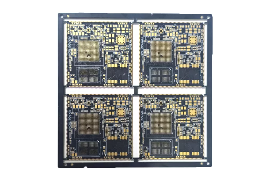
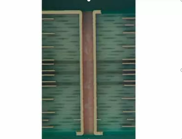
Representative sample: 8-layer FR-4 SY1000-2 construction, black solder mask, ENIG, 3/3 mil line/space and +/-7% impedance. These are sample-specific values, not blanket production limits.Microsection of a 20-layer multilayer PCB. No customer, application, yield or reliability result is inferred from this image.
Typical Multilayer PCB Applications
Communication, networking and intelligent-terminal equipment
Industrial control and instrumentation
Computing and data-processing hardware
Automotive and medical electronics subject to project-specific requirements
Aerospace and other high-reliability programs subject to qualification
Information Needed for a Multilayer PCB Quotation
Gerber, ODB++ or IPC-2581 data, NC drill files and a dimensioned fabrication drawing
Released layer stack-up, material category or exact grade, dielectric and copper thicknesses
Finished dimensions and thickness, via table, fill/cap rules and special-process notes
Single-ended/differential impedance table, reference layers, coupon and test requirements
Surface finish, solder mask, legend, panel delivery and inspection/report requirements
Prototype, pilot or production quantity, target date and shipping destination
Describe the key requirements in the Message field. Our team will confirm the file-transfer method for the complete manufacturing package after receiving the inquiry.
Send Your Multilayer PCB Project Details
Include the layer count, stack-up, material, copper, via structure, impedance requirements, quantity and target date. Our team will confirm the file-transfer method for the complete technical package.
Why Work with Benchuang for Multilayer PCBs
Benchuang supports multilayer PCB projects from stack-up and DFM review through prototype, pilot and production planning. Founded in 2007, the company operates an approximately 40,000 m2 Meizhou manufacturing center with nearly 500 employees. The Shenzhen team coordinates overseas quotations, technical communication and export support, while manufacturing review covers materials, lamination, via structures, controlled impedance, special processes and inspection requirements.
Frequently Asked Questions
What is Benchuang's maximum multilayer PCB layer count?
The stated capability is up to 32 layers for prototype/sample and 18 layers for production. Final approval depends on the complete stack-up, thickness, materials, copper, vias, panel plan and quantity.
What minimum line and space can be reviewed?
Minimum inner- and outer-layer line/space is 45/45 um for prototype/sample. Production values are 45/50 um, subject to copper, finish, feature density and the complete design.
Can multilayer PCBs use blind, buried or laser microvias?
Yes, these structures can be reviewed when the layer span, drill size, pads, fill/cap requirements and stacked or staggered arrangement are defined. Feasibility is confirmed from the complete stack-up and process route.
What controlled-impedance tolerance is available?
The stated tolerance is +/-9% for prototype/sample and +/-10% for production. The stack-up, trace geometry, finished copper, reference planes, coupon and test method must be agreed together.
What copper weights are available?
Inner-layer copper is stated at 0.33-5 oz for prototype/sample and 0.33-4 oz for production. Outer-layer copper is 0.33-5 oz for both; achievable line/space and plating must be evaluated with copper weight.
Which surface finishes are available?
Options include ENIG, OSP, OSP plus ENIG, ENEPIG and plated gold fingers. Selection depends on assembly, contact, storage and project-specific requirements.
What files are required for a multilayer PCB quotation?
Provide board and drill data, fabrication drawing, released stack-up, material and copper, via table, impedance requirements, finish, panel format, inspection criteria, quantities and target date.
What determines multilayer PCB lead time?
Material availability, stack-up approval, engineering-question closure, lamination and via complexity, panel layout, finish, special processes, testing and quantity determine the confirmed schedule.