IC Substrate PCB Project Review and Manufacturing Compatibility
IC package substrate feasibility depends on the package architecture, material system, build-up stack-up, fine-pitch routing, microvias, surface finish, warpage and assembly interfaces. Shenzhen Benchuang Precision Electronics Co., Ltd. confirms the manufacturing route, feature limits and qualification evidence only after reviewing the released project data.
IC Substrate Project Compatibility Review
Define the package architecture, material stack-up, fine geometry, microvia structure, warpage and assembly interfaces for project-specific review. Use the matrix below as a quotation checklist; feasibility is confirmed against the complete released design.
IC Substrate Project Compatibility Matrix
Manufacturing compatibility is confirmed for the complete project, not for an isolated feature. Approval depends on the combined package architecture, material system, build-up, fine geometry, microvia structure, dimensions, warpage, finish, test plan and order volume.
Qualification area
Required project definition
Package architecture
Define wire-bond or flip-chip interface, die/chiplet arrangement, bump or ball map and next-level assembly.
Material system
Specify exact maker/grade, core and build-up dielectrics, or coreless construction when applicable; state substitution rules.
Layer build-up
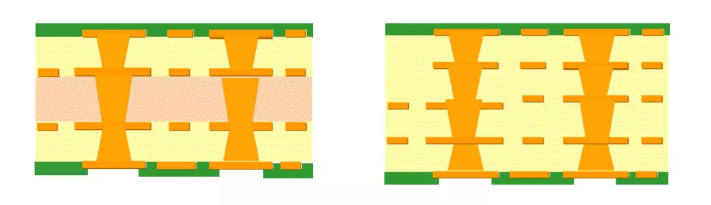
Release dielectric and copper thicknesses, layer relationships, reference structures and lamination sequence.
Line/space and pads
Provide target geometry, tolerances, pad sizes, registration requirements and critical areas.
Microvia structure
Define drill diameter, span, capture/target pads, stacked or staggered arrangement, fill and cap requirements.
Dimensions and thickness
Provide finished X/Y dimensions, total thickness, local thickness and datum/tolerance scheme.
Warpage and coplanarity
State the measurement condition, temperature, support method, limit and acceptance method.
Metallurgy/surface finish
Match the finish and metal stack to wire-bond, bump, solder or contact requirements.
Electrical performance
Define impedance, loss or frequency context, reference planes, coupon design and test method when required.
Inspection/qualification
Define electrical, dimensional, visual, microsection and reliability evidence plus pass/fail criteria.
IC Substrate Quotation Requirements
IC substrate requirements cannot be quoted reliably from an outline and layer count alone. The package architecture should identify the die, chiplet, bump, wire-bond, ball or land interfaces and the relationship between the package substrate and the next-level assembly. Release the exact material system, stack-up, routing and pad geometry, microvia structure, surface finish, finished dimensions, thickness, warpage and coplanarity requirements.
The quotation package should also define the electrical test method, impedance or loss requirements where applicable, inspection evidence, reliability conditions, acceptance criteria, prototype quantity and expected volume. Material availability and any allowed substitution must be agreed before the process route is approved.
Package Architecture and Build-Up Stack-Up
The package drawing should identify all interface types and the assembly sequence. Wire-bond and flip-chip designs create different pad, finish, routing, coplanarity and inspection needs. BGA, LGA, CSP and SiP projects also require the exact ball or land map, component-side and board-side interface definitions and any keep-out or mechanical constraints.
The released build-up should state every dielectric and copper layer, material grade, thickness target, copper treatment and lamination relationship. If an ABF, BT or another specified material system is required, provide the exact maker and grade plus permitted alternatives. Benchuang will confirm material and process compatibility for the individual project rather than applying a generic approval to all substrate constructions.
Fine-Pitch Routing, Microvias and Electrical Requirements
Fine routing must be evaluated together with pad dimensions, registration, copper thickness, imaging and etching, dielectric properties and the approved panel/process route. Do not rely on a generic line/space value from another package. Identify the critical layers and features directly in the data and fabrication notes.
For microvias, define the layer span, drill target, capture and target pads, stacked or staggered arrangement, filling, plating and capped-pad requirements. When impedance, loss or high-speed behavior is important, include the stack-up, trace geometry, reference structures, design basis, coupon and test method so the electrical requirement can be reviewed with manufacturing tolerances.
Surface Finish, Warpage and Qualification
Surface finish and metallurgy must suit the package assembly process, including soldering, wire bonding, bumping or other interface requirements. Provide the required metal stack, thickness range, exposed-pad geometry and verification method. A finish should not be selected by name alone when bonding or package reliability depends on the complete interface.
Warpage and coplanarity limits need a measurement condition and temperature because the result changes with construction, copper distribution and test setup. Define the finished limit, support method, temperature, sample size and acceptance rule. Qualification requirements may include dimensional and visual inspection, electrical test, microsection review, thermal or environmental testing and project-specific reports.
IC Substrate Project Types We Can Review
Wire-bond and flip-chip package substrate concepts
BGA, LGA, CSP and system-in-package interface requirements
Build-up and substrate-like PCB constructions
Fine-routing and microvia package-interface boards
The list describes project types that can enter compatibility review. It is not automatic approval of every material, feature combination, qualification class or volume. The manufacturing route is confirmed only after the complete technical package is evaluated.
Representative IC Substrate Images
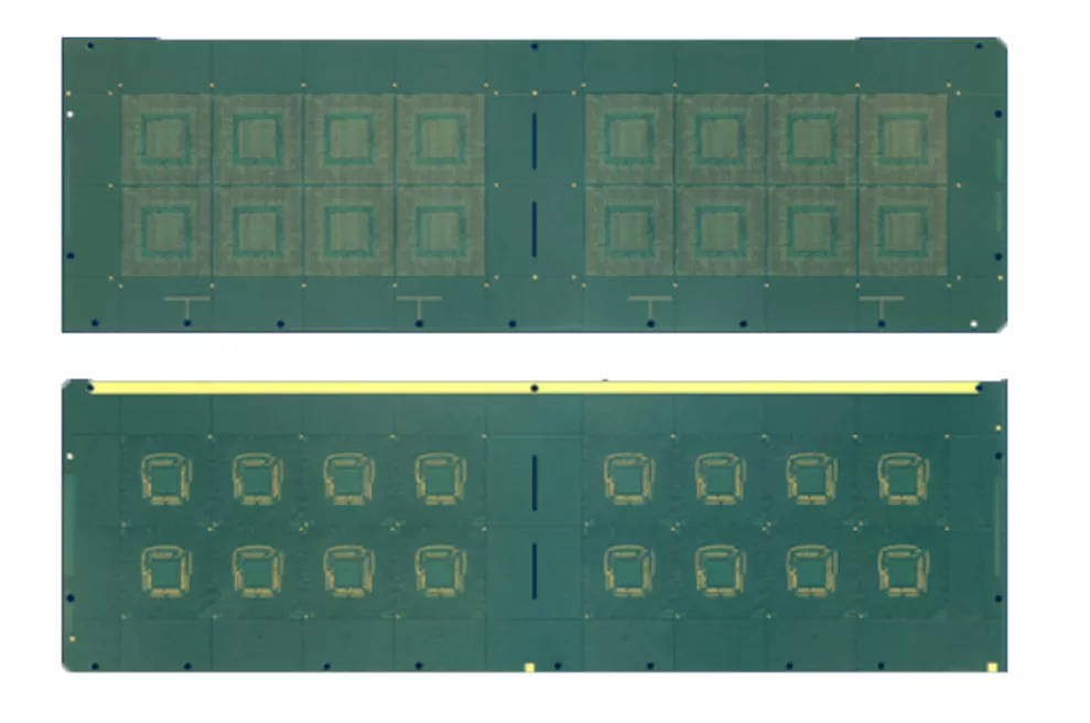
Precision IC substrate PCB. Literal project-category image; no unverified feature dimensions or package claims.Ultra-thin IC substrate PCB. No numeric thickness is inferred from the image name or appearance.
Information Needed for an IC Substrate Quotation
Package architecture drawing, interface map and Gerber, ODB++ or IPC-2581 manufacturing data
Exact material system, released build-up stack-up, copper and finished dimensions/thickness
Critical line/space, pad geometry, registration and microvia construction
Surface finish/metallurgy, warpage and coplanarity limits with measurement conditions
Electrical, inspection, reliability and qualification requirements with acceptance criteria
Prototype and expected production quantity, target date and shipping destination
Describe the key requirements in the Message field. Our engineering and sales teams will review the inquiry and confirm the secure file-transfer method for the complete package.
Send Your IC Substrate Project Details
Include the package architecture, material system, build-up, critical features, warpage requirements, quantity and target date. Our team will confirm the file-transfer method for the complete technical package.
Why Work with Benchuang for IC Substrate Project Review
Benchuang uses an engineering-led qualification process for IC substrate and substrate-like PCB inquiries. Package architecture, materials, build-up, fine geometry, microvias, finish, warpage and test requirements are reviewed together before a manufacturing route is confirmed. The Meizhou production team and Shenzhen overseas-support team coordinate technical questions, quotation inputs and export communication, giving international buyers a clear decision path without unsupported blanket capability claims.
Frequently Asked Questions
How is an IC substrate different from a system PCB?
An IC substrate forms the fine electrical and mechanical interface between the semiconductor package and the next assembly level. It normally has package-specific pad, routing, material, warpage, finish and qualification requirements beyond those of a general system PCB.
What data is required for an IC substrate quotation?
Provide the package architecture, interface map, manufacturing data, material system, build-up, fine geometry, microvias, dimensions, thickness, warpage, finish, electrical tests, qualification criteria, quantities and target date.
Can Benchuang review ABF or BT material requirements?
Yes, project requirements using ABF, BT or another specified system can be reviewed. Provide the exact maker and grade, construction and permitted substitutions; material availability and manufacturing compatibility must be confirmed for the project.
What is the minimum IC substrate line/space capability?
There is no single value that should be applied to every package. The achievable geometry depends on the material, copper, layer, pad and registration requirements, imaging/etch route, panel plan and qualification criteria, so it is confirmed from the released package.
How should warpage and coplanarity be specified?
State the finished limit, measurement temperature, support or fixture method, datum, sample condition and acceptance rule. These conditions are required because construction and test setup affect the measured result.
How is the surface finish selected?
The metal stack must match the assembly interface, such as wire bonding, soldering, bumps or contact areas. Include required thicknesses, pad geometry and verification method rather than selecting a generic finish by name alone.
What inspection or qualification evidence can be requested?
Define the required dimensional, visual, electrical, microsection, thermal, environmental or project-specific reports and pass/fail criteria in the quotation package. Availability and scope are confirmed with the manufacturing route.
Can prototype and production volumes be supported?
Prototype and expected volume can both enter project review. The approved scope, schedule and production route are confirmed only after material, feature combination, qualification plan and capacity requirements are evaluated.